Semiconductor integrated circuit device

a technology of integrated circuits and semiconductors, applied in semiconductor devices, semiconductor/solid-state device details, electrical apparatuses, etc., can solve the problems of increasing chip size, reducing cell efficiency, and difficult manufacturing of 1t-1c drams with memory cells smaller than 0.1 m in design rules

Inactive Publication Date: 2005-04-19
KK TOSHIBA
View PDF6 Cites 58 Cited by
  • Summary
  • Abstract
  • Description
  • Claims
  • Application Information

AI Technical Summary

Problems solved by technology

1T-1C DRAMs having memory cells reduced in design rule to smaller than 0.1 μm are difficult to manufacture.
The DRAM including sense amplifier circuits for individual bit line BL decreases the cell efficiency and increases in chip size because the sense amplifier circuits occupy a large area.
This means that FBC will lose its advantage of having a smaller cell size than 1T-1C type DRAM.

Method used


Image

  • Semiconductor integrated circuit device
  • Semiconductor integrated circuit device
  • Semiconductor integrated circuit device

Examples


first embodiment

(First Embodiment)

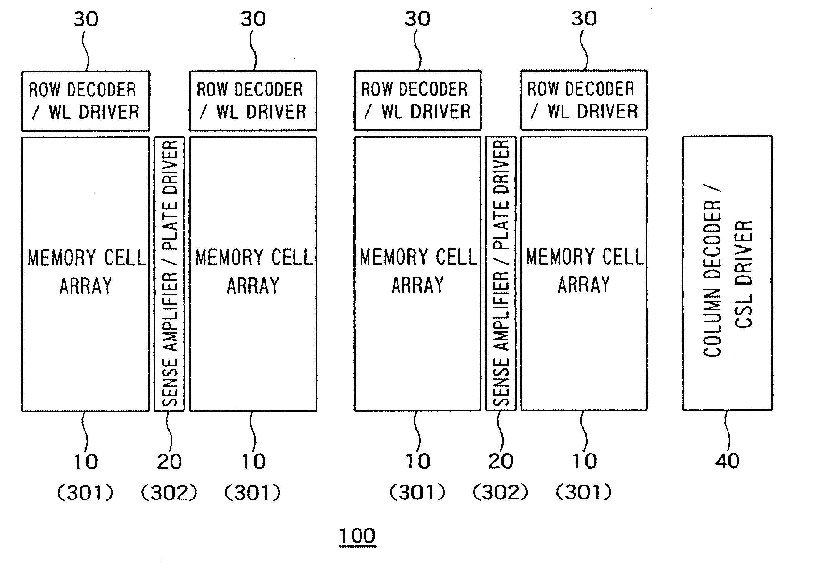
[0033]FIG. 1 is a block diagram showing a memory portion of DRAM 100 according to the first embodiment of the invention. The memory portion includes memory cell arrays 10, sense amplifier / plate driver portions (herein below simply called SA / PDs) 20, row decoders combined with WL drivers (herein below simply called row decoders) 30, and a column decoder combined with CSL (column select line) driver (herein below simply called column decoder) 40.

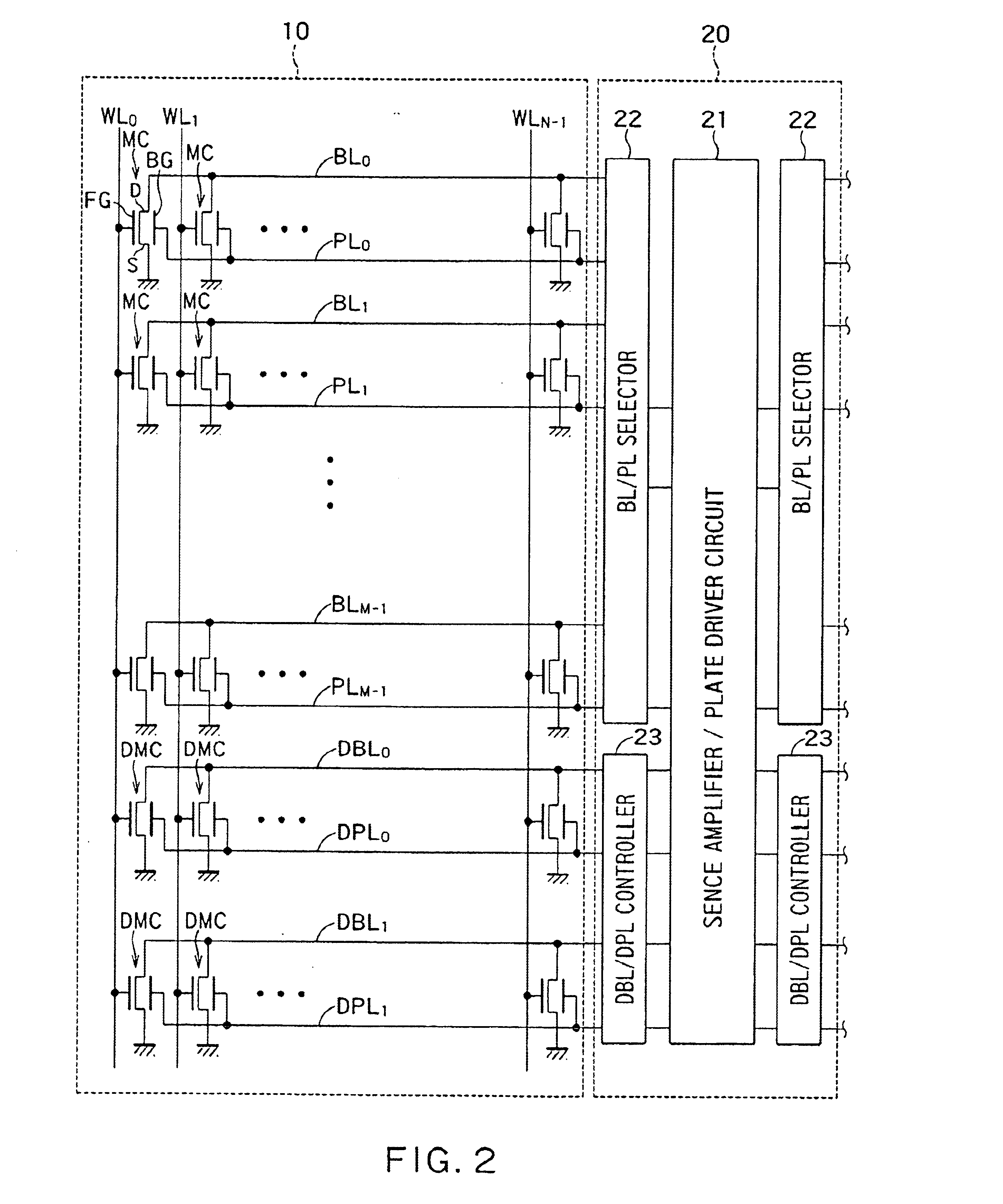
[0034]Each memory cell 10 comprises memory cells having a matrix arrangement of FBCs. The plurality of memory cell arrays 10 are aligned side by side. The SA / PDs 20 are provided in every other spaces between memory cell arrays 10. One SA / PD 20 is connected to memory cell arrays 10 at both sides thereof and can detect and latch data in these memory cell arrays 10. In addition, the SA / PD 20 can selectively control the potential of the plate lines PL shown in FIG. 2 and can drive the selected plate line PL.

[0035]Each row decoder...

second embodiment

(Second Embodiment)

[0068]FIG. 7 is a block diagram showing the memory portion of DRAM 200 according to the second embodiment of the invention. In this embodiment, the sense amplifier portion 26 and the plate driver portion 28 are provided in separate locations. The other structural features of this embodiment are identical to those of the first embodiment. They are, therefore, not explained here.

[0069]The sense amplifier portion 26 is located near one side of the memory cell array 10. The plate driver portion 28 is located near the opposite side of the memory cell array 10 to be opposed to the sense amplifier portion 26 via the memory cell array 10. As such, the sense amplifier portion 26 and the plate driver portion 28 are provided to appear alternately in spaces between every two adjacent memory cell arrays 10, and they each are commonly used for two memory cell arrays 10 at both sides thereof.

[0070]FIG. 8 is a circuit diagram showing one memory cell array 10, one sense amplifier ...

third embodiment

(Third Embodiment)

[0075]FIG. 9 is a cross-sectional view of the memory portion of DRAM 300 according to the third embodiment of the invention, taken along a word line WL. When the DRAM 300 is cut along a BL line, it will appear identical to FIG. 3. The cross-sectional view of FIG. 9 may be same as the cross-sectional view taken along the X—X line of FIG. 3.

[0076]As shown in FIG. 9, each plate line PL in this embodiment is associated with four bit lines BL and four body regions 160. A simulation of operation of the DRAM 300 results identical to that of the first embodiment under the same conditions.

[0077]According to the instant embodiment, even when there is a difficulty in forming the plate lines PL in a fine pitch arrangement, or in forming the plate lines PL in precise alignment with the bit line BL, the plate line PL can be formed in parallel with the bit lines BL.

[0078]In this embodiment, however, if data “0” is written in a memory cell in the same manner as the first and secon...


PUM


Abstract

A semiconductor integrated circuit device comprises a semiconductor substrate; an insulating layer formed on the semiconductor substrate; a semiconductor layer insulated from the semiconductor substrate by the insulating layer; source regions of a first conduction type and drain regions of the first conduction type both formed in the semiconductor layer; body regions of a second conduction type formed in the semiconductor layer between the source regions and the drain regions to store data by accumulating or releasing an electric charge; word lines formed on the body regions in electrical isolation from the body regions to extend in a first direction; bit lines connected to the drain regions and extending in a direction different from the first direction; and buried wirings formed in the insulating layer in electrical isolation from the semiconductor substrate and the semiconductor layer, said buried wirings extending in parallel with the bit lines.

Description

CROSS-REFERENCE TO RELATED APPLICATIONS[0001]This application is based upon and claims the benefit of priority from the prior Japanese Patent Application No. 2003-370696, filed on Oct. 30, 2003, the entire contents of which are incorporated herein by reference.BACKGROUND OF THE INVENTION[0002]1. Field of the Invention[0003]The present invention relates to a semiconductor integrated circuit device.[0004]2. Related Background Art[0005]For years, 1T-1C (1 transistor 1 capacitor) DRAM (dynamic random access memory) devices have been manufactured. 1T-1C DRAMs having memory cells reduced in design rule to smaller than 0.1 μm are difficult to manufacture.[0006]On this account, a DRAM having FBCs (floating body cells) as shown in FIG. 12 has been proposed (Japanese Patent Laid-open Publication No. JP2002-246571). FBC comprises a FET (field effect transistor) formed in SOI. The gate G of the FET is connected to a word line WL, the drain D is connected to b bit line BL, and the source S is co...

Claims


Application Information

Patent Timeline
Patent Type & Authority Patents(United States)
IPC IPC(8): H01L21/70H01L29/66H01L21/8242H01L21/3205H01L21/02H01L29/786H01L27/108H01L27/01H01L23/52H01L27/02H01L27/12
CPCH01L27/108H01L29/78648H01L29/7841H01L27/1203H01L27/0207H10B12/00
Inventor OHSAWA, TAKASHI
Owner KK TOSHIBA
Why Eureka
Try Eureka