Multi-chip module and method for forming and method for deplating defective capacitors

a technology of defective capacitors and chip capacitors, applied in the field of multi-chip modules, can solve the problems of increasing the signal run length, consuming valuable area, and reducing the effect of surface mount and chip capacitors to marginal and unacceptable levels, and achieve the effect of reducing the thickness of the semiconductor substra

Inactive Publication Date: 2005-04-19
FUJITSU LTD
View PDF67 Cites 102 Cited by
  • Summary
  • Abstract
  • Description
  • Claims
  • Application Information

AI Technical Summary

Problems solved by technology

However, as the operating frequency of MCMs has increased, the effectiveness of these surface mount and chip capacitors has decreased to marginal and unacceptable levels.
Unfortunately, staggering the via structures can consume valuable area in a multilayer circuit structure and can increase the signal run length.
This can decrease the density of the circuitry in a multilayer circuit structure.
Open circuits can form if the coating is not thick enough or is not uniform.
Microelectric devices are rendered unrecognizable and may be destroyed by means of an electrochemical reaction comprising an electro-chemical or chemical etching and / or de-plating process.

Method used


Image

  • Multi-chip module and method for forming and method for deplating defective capacitors
  • Multi-chip module and method for forming and method for deplating defective capacitors
  • Multi-chip module and method for forming and method for deplating defective capacitors

Examples


Embodiment Construction

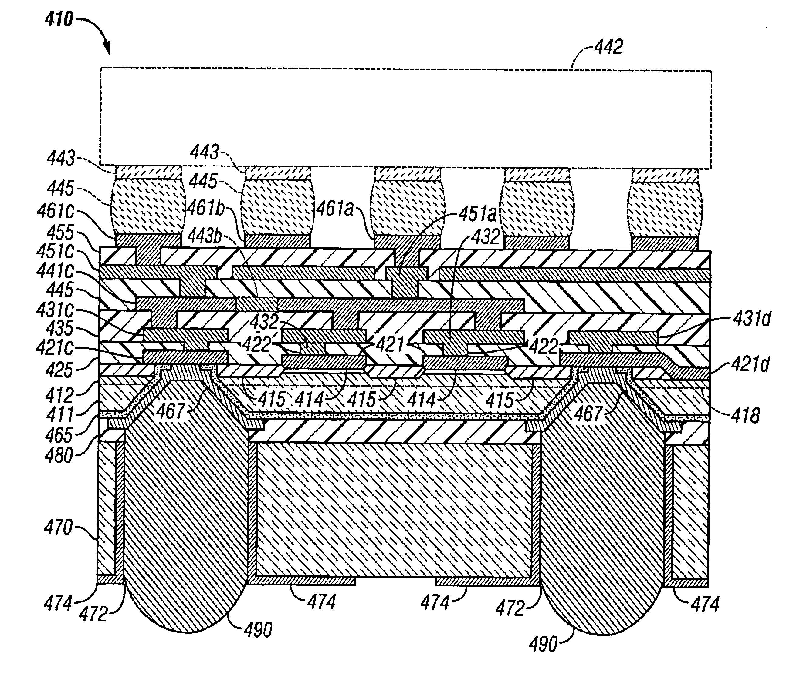
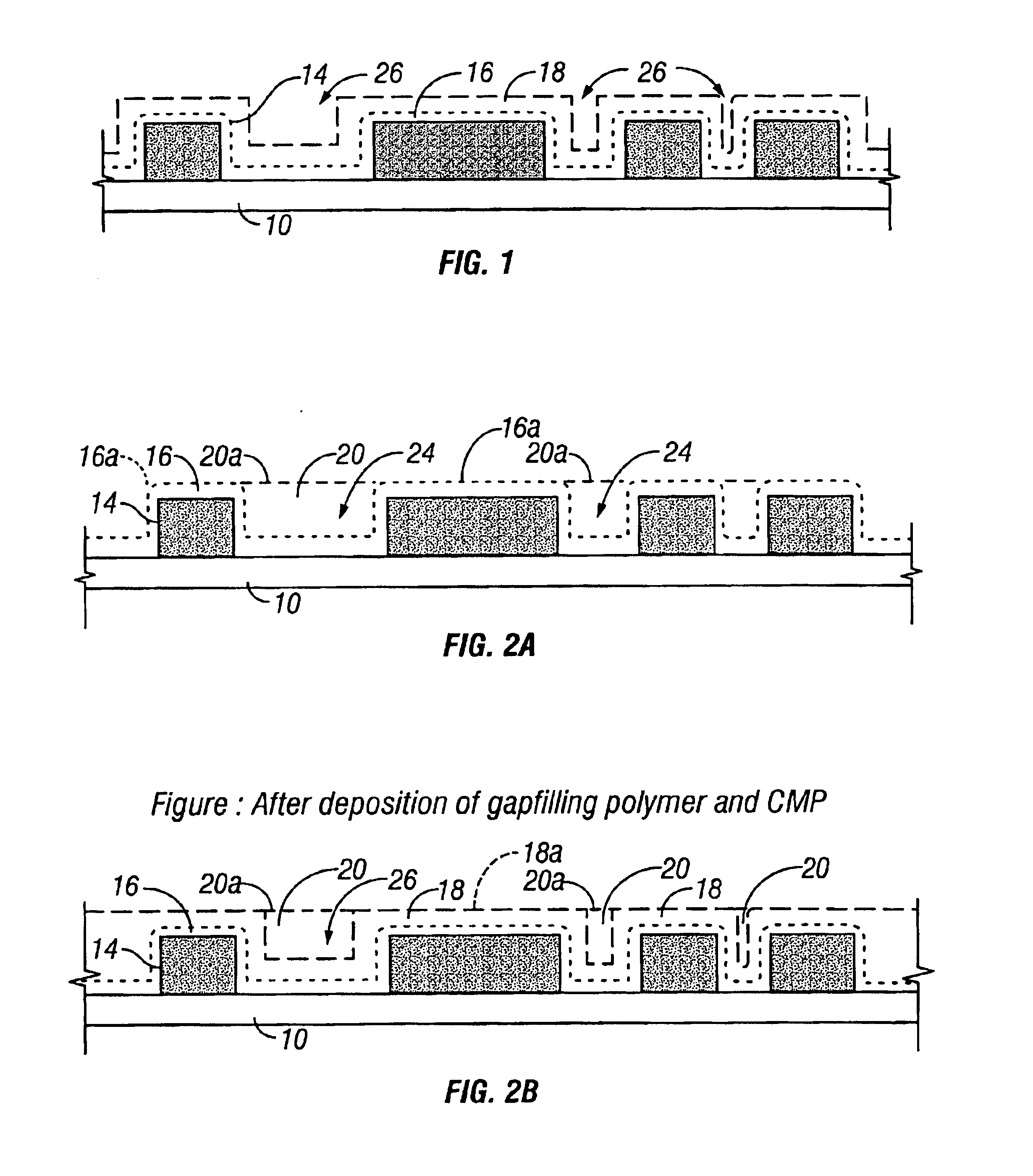
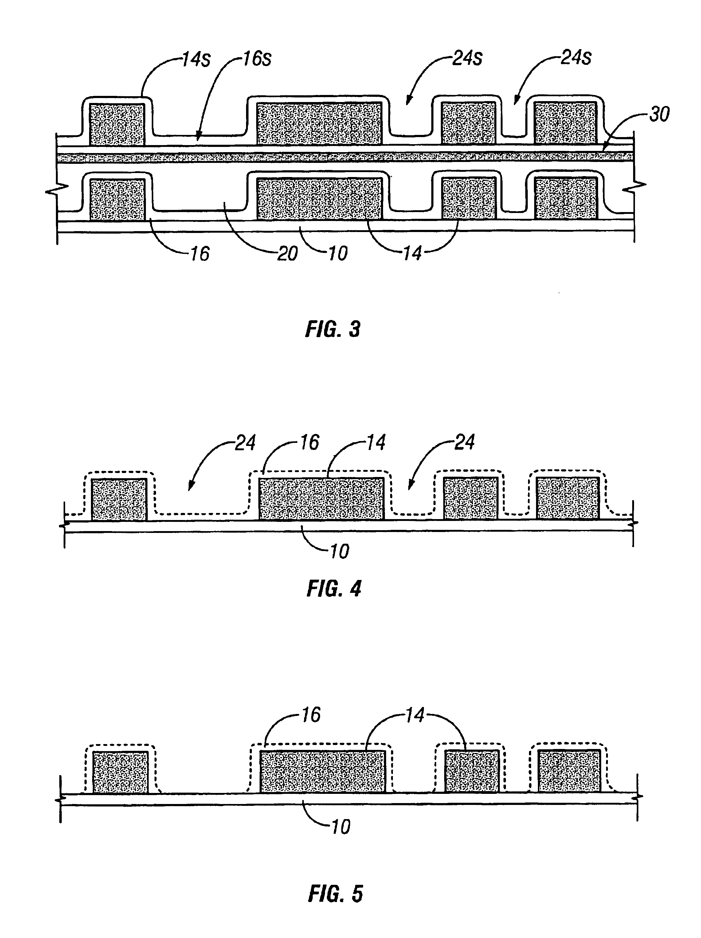
[0104]Referring in detail now to the drawings, there is seen in FIGS. 1-22 various embodiments of a structure and method for making a low dielectric constant MCM. Structures and methods of the type illustrated in FIGS. 1-22 are of priority of future generation MCM's as they will enable gigahertz speed products without huge losses, noise, and delays. The advantages of a low dielectric constant MCM of the various embodiments of the present invention are: (1) higher performance MCMs may be made with lower dielectric constants; (2) reduces amount of chemical mechanical polishing (CMP) required by using only conformal dielectric coatings in the MCMs; (3) enables better dielectric-layer adhesion than possible with only one type of dielectric polymer because of using two or more dielectric polymers; and (4) enables controlled impedance structures. A dielectric constant is a value serving as an index of the ability of the dielectric material(s) (e.g., polymers) to resist the transmission of...


PUM


Abstract

A method for deplating defective capacitors comprising forming a plurality of capacitors on a semiconductor substrate, forming a plurality of metal contacts on the plurality of capacitors, and depositing a layer of photoresist on the semiconductor substrate. The photoresist layer is patterned so that the plurality of metal contacts are exposed, which are then contacted with an electrically conductive solution. The metal contacts, which are disposed over defective capacitors, are subsequently deplated. A method for forming a multi-chip module comprising forming a thin-film polymeric interconnect structure having a pair of sides, one of which is disposed on a silicon substrate having active or passive devices and the other of which has a computer chip mounted thereon. A multi-chip module formed by the method.

Description

[0001]This is a continuation-in-part patent application of patent applications having Ser. No. 09 / 429,854, filed Oct. 28, 1999, now U.S. Pat. No. 6,428,942, and Ser. No. 09 / 956,605, filed Sep. 18, 2001. Benefit of the earlier filing dates is claimed for all common subject matter.BACKGROUND OF THE INVENTION[0002]1. Field of the Invention[0003]The present invention is related to multichip modules (MCMs). More specifically, the present invention provides MCM substrates, as well as to a method for making multichip module substrates and to a method for deplating defective capacitors.[0004]2. Description of the Prior Art[0005]Multilayer circuit structures can be used to electrically communicate two or more electrical devices such as two or more computer chips. Multilayer circuit structures typically contain multiple conductive layers separated by one or more dielectric layers. Via structures disposed in apertures in the dielectric layers provide conductive paths so that electrical signals...

Claims


Application Information

Patent Timeline
Patent Type & Authority Patents(United States)
IPC IPC(8): H01L21/48H01L21/02H05K3/46H05K3/00H05K3/10H05K3/24
CPCH01L21/486H01L24/96H05K3/4647H01L2221/68345H01L2221/68359H01L2224/1308H01L2224/13082H01L2224/13109H01L2224/13111H01L2224/13144H01L2224/13147H01L2224/16237H01L2924/01004H01L2924/01013H01L2924/01027H01L2924/01029H01L2924/0103H01L2924/01042H01L2924/01046H01L2924/01047H01L2924/01051H01L2924/01074H01L2924/01075H01L2924/01078H01L2924/01079H01L2924/01082H01L2924/01322H01L2924/01327H01L2924/14H01L2924/15311H01L2924/19041H01L2924/30105H01L2924/30107H01L2924/3011H05K3/0035H05K3/108H05K3/243H05K3/4602H05K2203/066H05K2203/0733H05K2203/1383H01L2224/81193H01L2224/81141H01L2924/00013H01L2924/01005H01L2924/01006H01L2924/01019H01L2924/01023H01L2924/01024H01L2924/01033H01L2924/01072H01L2224/16501H01L2224/81191H01L2924/00014H01L2924/01049H01L2224/13099H01L2924/15787H01L2924/12042H01L2224/05573H01L2224/05568H01L2224/13023H01L2924/00H01L2224/05599
Inventor MASSINGILL, THOMAS J.MCCORMACK, MARK THOMASWANG, WEN-CHOU VINCENT
Owner FUJITSU LTD
Why Eureka
Try Eureka