
Input/output buffer

a buffer and input technology, applied in the field of input/output buffer, can solve the problems of increasing circuit complexity, requiring more wafer area, and unable to meet the requirements of 3.3v devices, so as to prevent unneeded current leakage

Inactive Publication Date: 2005-04-19
FARADAY TECH CORP
View PDF4 Cites 0 Cited by
  • Summary
  • Abstract
  • Description
  • Claims
  • Application Information

AI Technical Summary

Benefits of technology

The solution effectively prevents undesired current leakage by dynamically adjusting the N-well region voltage, ensuring compatibility with higher input logic signals and reducing circuit complexity by eliminating the need for external control signals.

Problems solved by technology

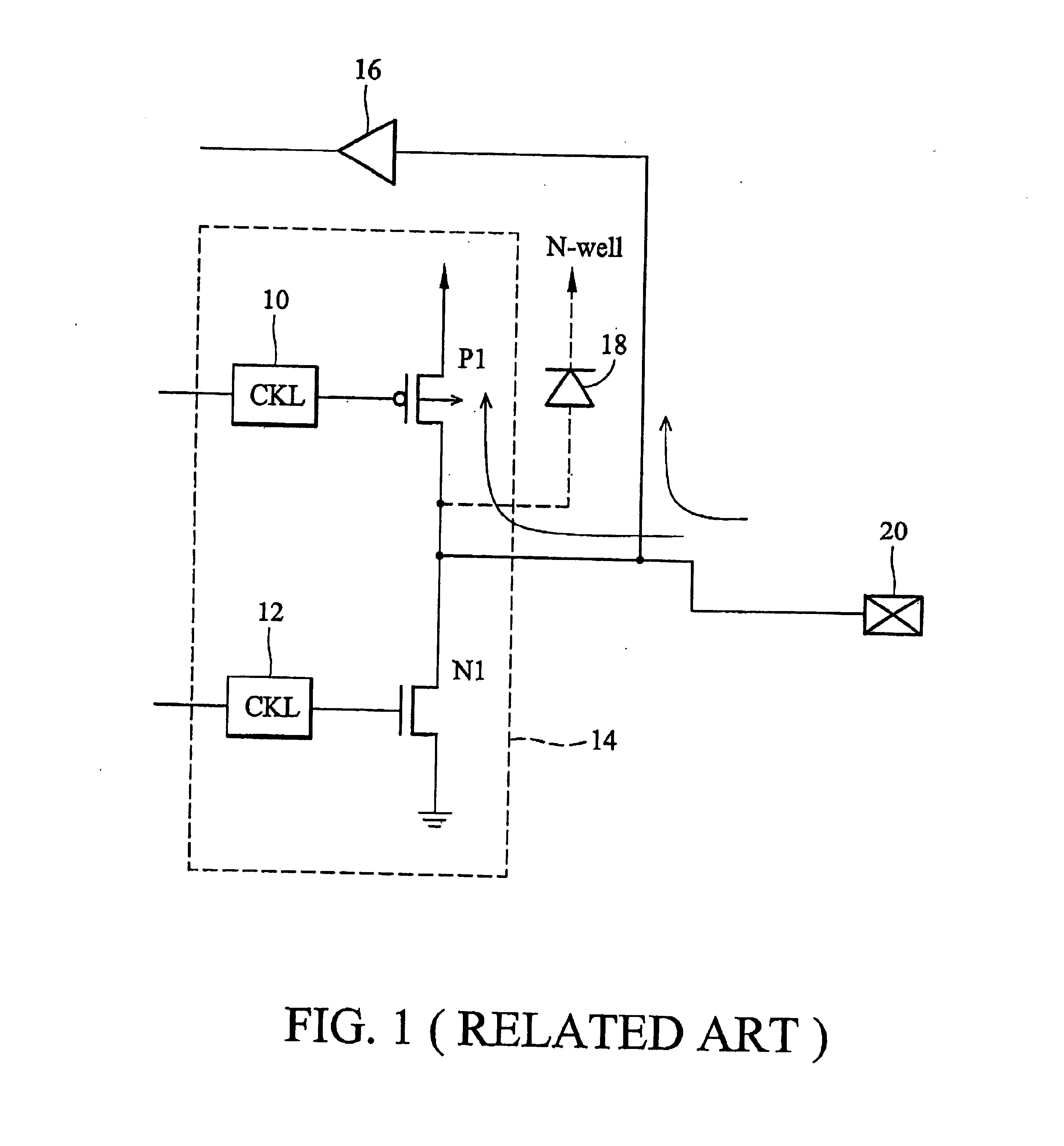
Compatibility between the new 3.3V devices and the older 5V devices can thus be a problem.
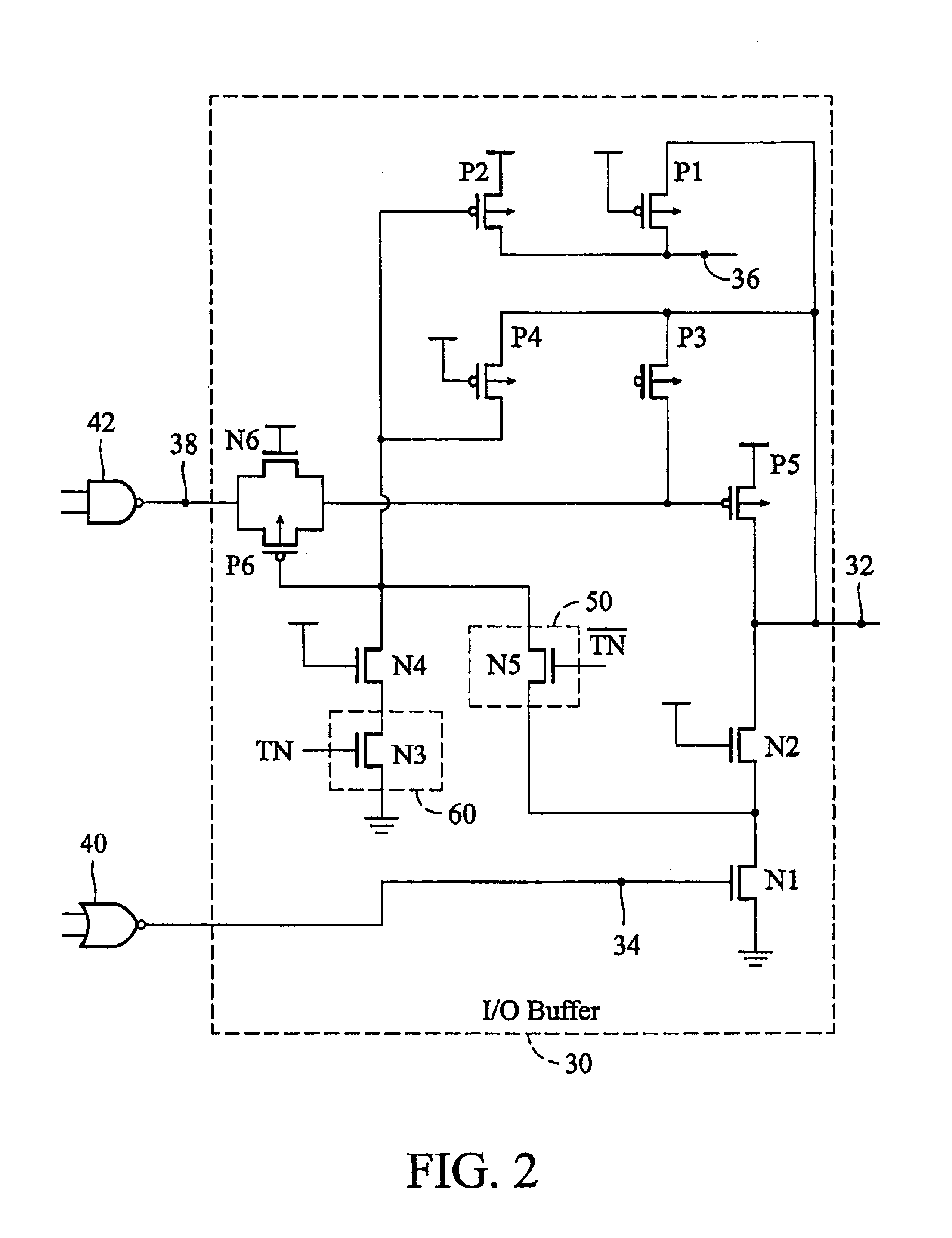
However, this I / O buffer needs two external control signals TN and / TN from the core circuits (not shown) to control the voltage at the floating N-well region being above 3.3V, increasing circuit complexity and requiring more wafer area.

Method used


Image

  • Input/output buffer
  • Input/output buffer
  • Input/output buffer

Examples


Embodiment Construction

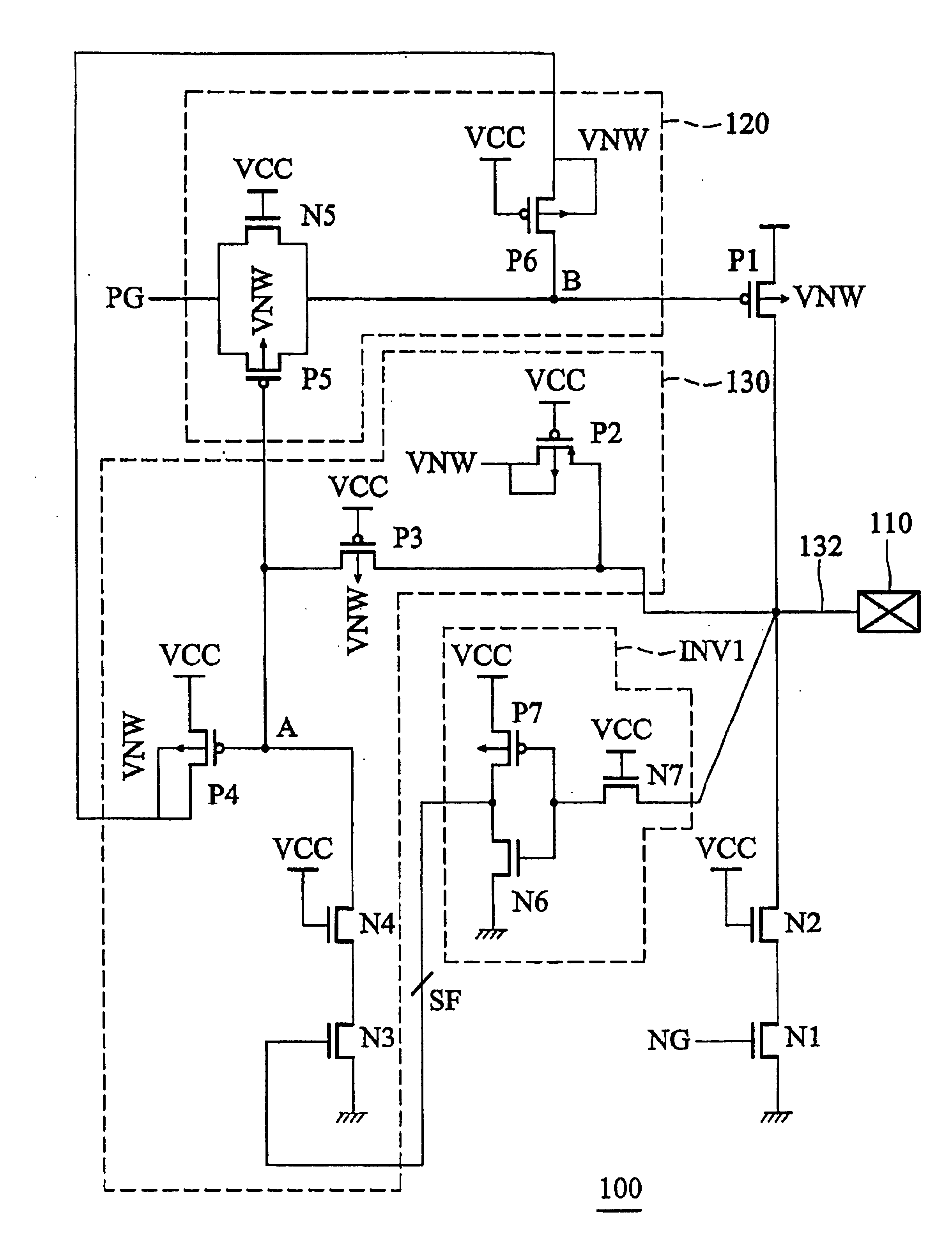
[0019]FIG. 3 is a diagram of the input / output buffer 100 according to the present invention. This I / O buffer 100 is capable of accepting an input logic signal higher in voltage level than the system voltage VCC. In the following embodiment of the present invention, the system voltage VCC is 3.3V, and the input logic signal switches between 0V and 5V, wherein the 5V high-voltage logic state is higher in voltage level than the system voltage VCC of 3.3V. However, it is to be understood that the invention is not limited to this embodiment.

[0020]As shown in FIG. 3, the input / output buffer includes an I / O circuit 140, a P-gate control circuit 120, an N-well control circuit 130, and a feedback detection device. In the present invention the feedback detection device can be an inverter INV1. The I / O circuit 140 has a PMOS transistor P1 and two NMOS transistors N1 and N2, and has an I / O port 132 coupled to an I / O pad. The PMOS transistor P1 has a floating N-well region, and a drain of the fi...


PUM


Abstract

An input / output buffer. An input / output circuit has a transmission terminal coupled to an I / O pad, and a floating N-well region. A P-gate control circuit conveys the second gate control signal to the gate of the first PMOS transistor. A feedback detection device is coupled between the transmission terminal and an N-well control circuit to output a feedback signal according to an input voltage at the I / O pad. The N-well control circuit adjusts the voltage level at the N-well region of the first PMOS transistor according to the feedback signal output from the feedback detection device.

Description

BACKGROUND OF THE INVENTION[0001]1. Field of the Invention[0002]The present invention relates to an input / output buffer, and more particularly, to an input / output buffer capable of accepting an input logic signal voltage higher than the system voltage.[0003]2. Description of the Related Art[0004]Conventionally, most IC devices are driven by a system voltage in the range of 0-5V. In these IC devices, high-voltage logic signals are set at the system voltage and low-voltage logic signals at the ground voltage. With advances in semiconductor technology, however, the system voltage can be reduced to 3.3V because the gate oxide layers in the IC device are thinner. Still lower system voltage may be possible in the future. In practice, however, an New 3.3V IC device is usually used in conjunction with older 5V peripheral devices. For instance, an New 3.3V VGA (video graphic adapter) may be used in conjunction with other older 5V peripheral devices in a personal computer. Compatibility betwe...

Claims


Application Information

Patent Timeline
Patent Type & Authority Patents(United States)
IPC IPC(8): H03K19/003
CPCH03K19/00315
Inventor CHEN, SHENG-HUACHANG, HUNG-YIWU, JENG-HUANG
Owner FARADAY TECH CORP
Learn More