Active matrix display device
a display device and active matrix technology, applied in the direction of identification means, instruments, discharge tubes, etc., can solve the problem of low productivity
- Summary
- Abstract
- Description
- Claims
- Application Information
AI Technical Summary
Benefits of technology
Problems solved by technology
Method used
Image

Examples
first embodiment
(Overall Configuration)
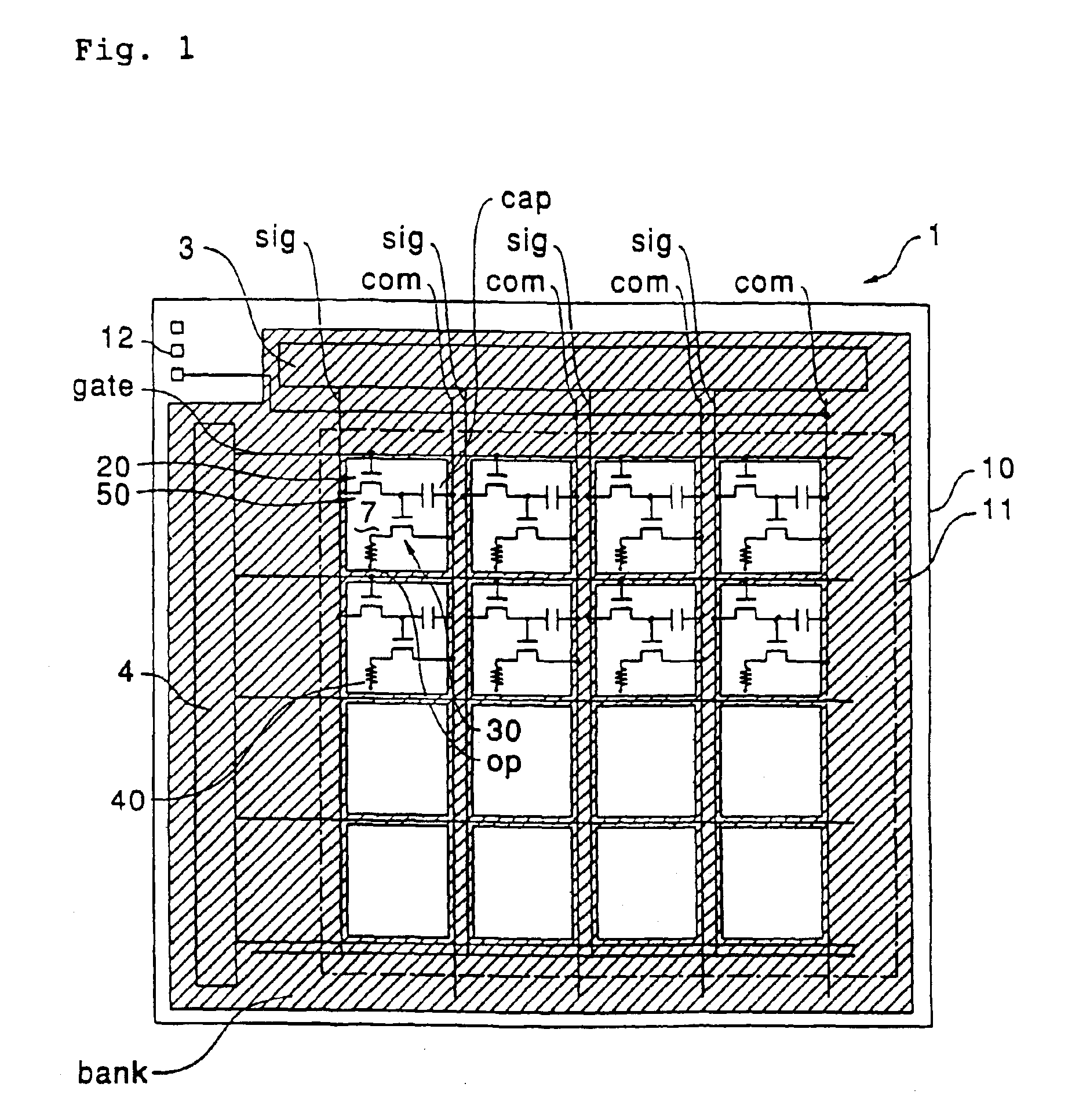
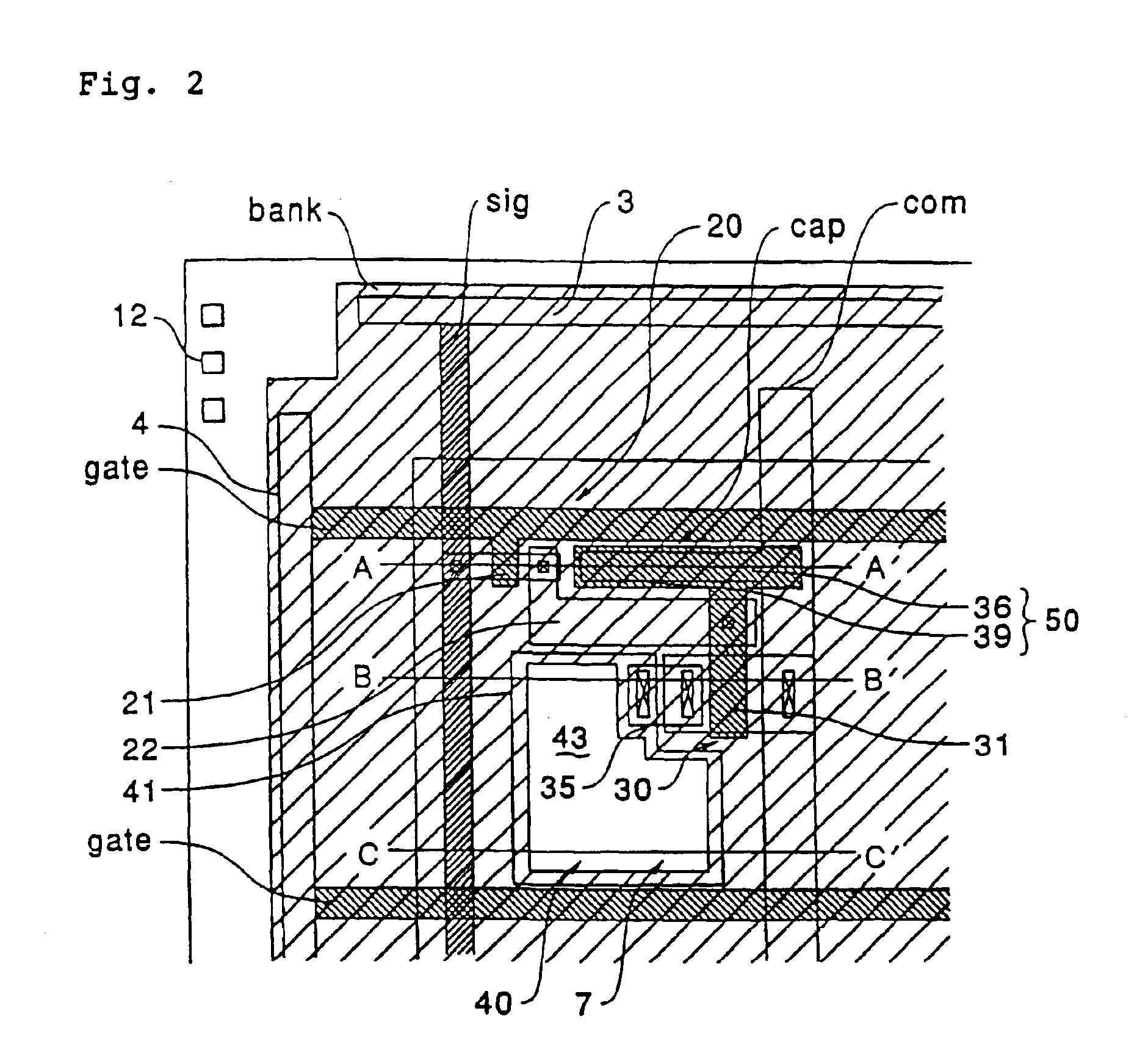
[0064]FIG. 1 is a schematic block diagram of an overall layout of an active matrix display device in accordance with the present invention. FIG. 2 is a plan view of a pixel extracted therefrom. FIGS. 3(A), 3(B) and 3(C) are cross-sectional views taken from line A-A′, B-B′, and C-C′, respectively, in FIG. 2.
[0065]In the active matrix display device 1 shown in FIG. 1, the central portion of a transparent substrate 10 as a base is used as a display section 11. Among a periphery of the transparent substrate 10, a data line driving circuit 3 that outputs image signals is provided on the ends of data lines sig, whereas a scanning line driving circuit 4 that outputs scanning signals is provided on the ends of scanning lines gate.
[0066]In these driving circuits 3 and 4, an n-TFT and a p-TFT form a complementary TFT, and many complementary TFTs form a shift resistor circuit, a level shifter circuit, and an analog switch circuit. In the display section 11, like in an ac...
second embodiment
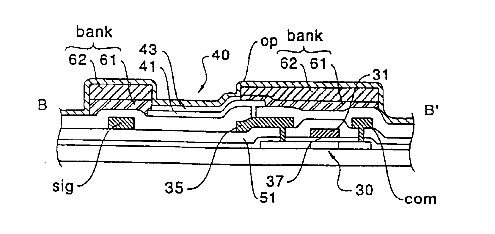
[0099]FIGS. 4(A), 4(B) and 4(C) are cross-sectional views of an active matrix display device in accordance with this embodiment at positions corresponding to line A-A′, B-B′, and C-C′, respectively, in FIG. 2. This embodiment has a basic configuration which is substantially the same as that of the first embodiment; hence, the same symbols are assigned for the same parts, without detailed description thereof. Since the region that forms the bank layer bank in the active matrix display device of this embodiment is the same as that in the first embodiment, FIGS. 1 and 2 are also referred to in the following description.
[0100]In order to prevent formation of a large parasitic capacitance in a data line sig, also, in this embodiment, as shown in FIGS. 1, 2, 4(A), 4(B), and 4(C), an insulating film (a bank layer bank, the region shaded with lines slanting downward to the left or double slanting lines at a wide pitch) which is thicker than an organic semiconductive film 43 is provided alon...
third embodiment
[0107]An active matrix display device 1 in this embodiment has the same configuration as that in the second embodiment, but a material for the bank layer bank is different. Thus, the same symbols are assigned for the same parts, without detailed description thereof. FIGS. 1, 2, 4(A), 4(B) and 4(C) are also referred to in the following description, as in the second embodiment.
[0108]In order to prevent formation of a large parasitic capacitance in a data line sig, as shown in FIGS. 1, 2, 4(A), 4(B), and 4(C), an insulating film (a bank layer bank, the region shaded with lines slanting downward to the left or double slanting lines at a wide pitch) which is thicker than an organic semiconductive film 43 is provided along the data line sig and a scanning line gate, and an opposite electrode op is formed above the bank layer bank.
[0109]The bank layer bank includes an inorganic lower insulating layer 61, such as a silicon nitride film, which is thicker than the organic semiconductive film ...
PUM
 Abstract
Description
Claims
Application Information
 - Generate Ideas
- Intellectual Property
- Life Sciences
- Materials
- Tech Scout
- Unparalleled Data Quality
- Higher Quality Content
- 60% Fewer Hallucinations
Browse by: Latest US Patents, China's latest patents, Technical Efficacy Thesaurus, Application Domain, Technology Topic, Popular Technical Reports.
© 2025 PatSnap. All rights reserved.Legal|Privacy policy|Modern Slavery Act Transparency Statement|Sitemap|About US| Contact US: help@patsnap.com