Microconverter and laminated magnetic-core inductor

a technology of laminated magnetic core and microconverter, which is applied in the direction of sustainable manufacturing/processing, semiconductor/solid-state device details, instruments, etc., can solve the problems of difficult inductor miniaturization, electronic parts, difficult miniaturization of inductor, etc., to achieve the effect of enhancing the functional value of electronic devices and reducing the size of inductor

Inactive Publication Date: 2005-04-26
FDK CORP
View PDF6 Cites 25 Cited by
  • Summary
  • Abstract
  • Description
  • Claims
  • Application Information

AI Technical Summary

Benefits of technology

[0009]Accordingly, it is an object of the present invention to provide a microconverter capable of being mounted in a small area on a SM circuit board and of enabling the miniaturization and functional enhancement of electronic devices including portable telephones.
[0010]Another object of the present invention is to provide techniques capable of providing a small, thin magnetic-core laminated inductor formed by laminating insulating magnetic layers and conductive pattern layers, capable of securing a wide linear range of variation of magnetic flux density and suitable for use in which direct currents are superposed.

Problems solved by technology

Although the IC having a comparatively high power capacity, i.e., one of the two principal components of the microconverter, is sufficiently miniaturized by fine processing techniques for fabricating semiconductor devices, it is difficult to miniaturize the inductor, particularly, the inductor included in a power unit, not to speak of forming the inductor in an IC.
Therefore, the inductor is difficult, as compared with other electronic parts, to miniaturize and to form in a small thickness.

Method used


Image

  • Microconverter and laminated magnetic-core inductor
  • Microconverter and laminated magnetic-core inductor
  • Microconverter and laminated magnetic-core inductor

Examples


first embodiment

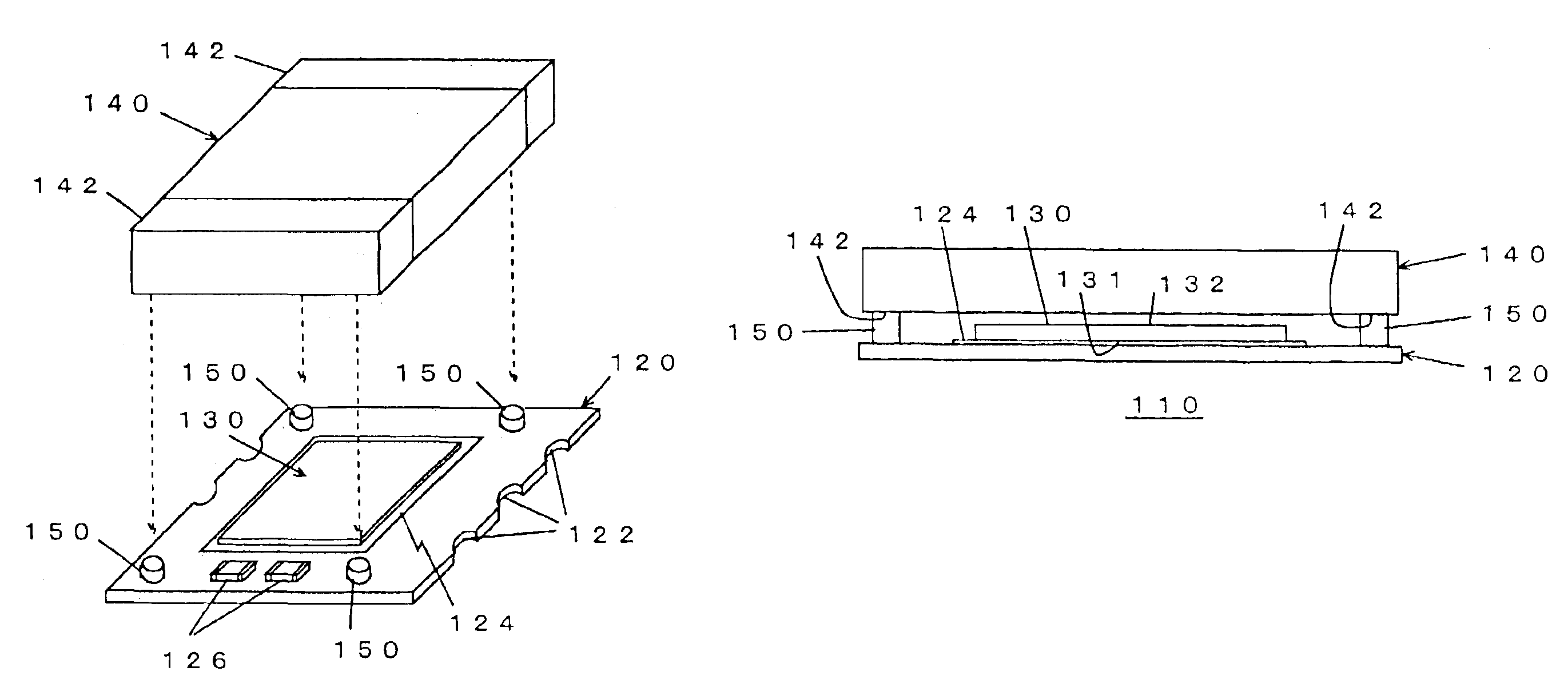
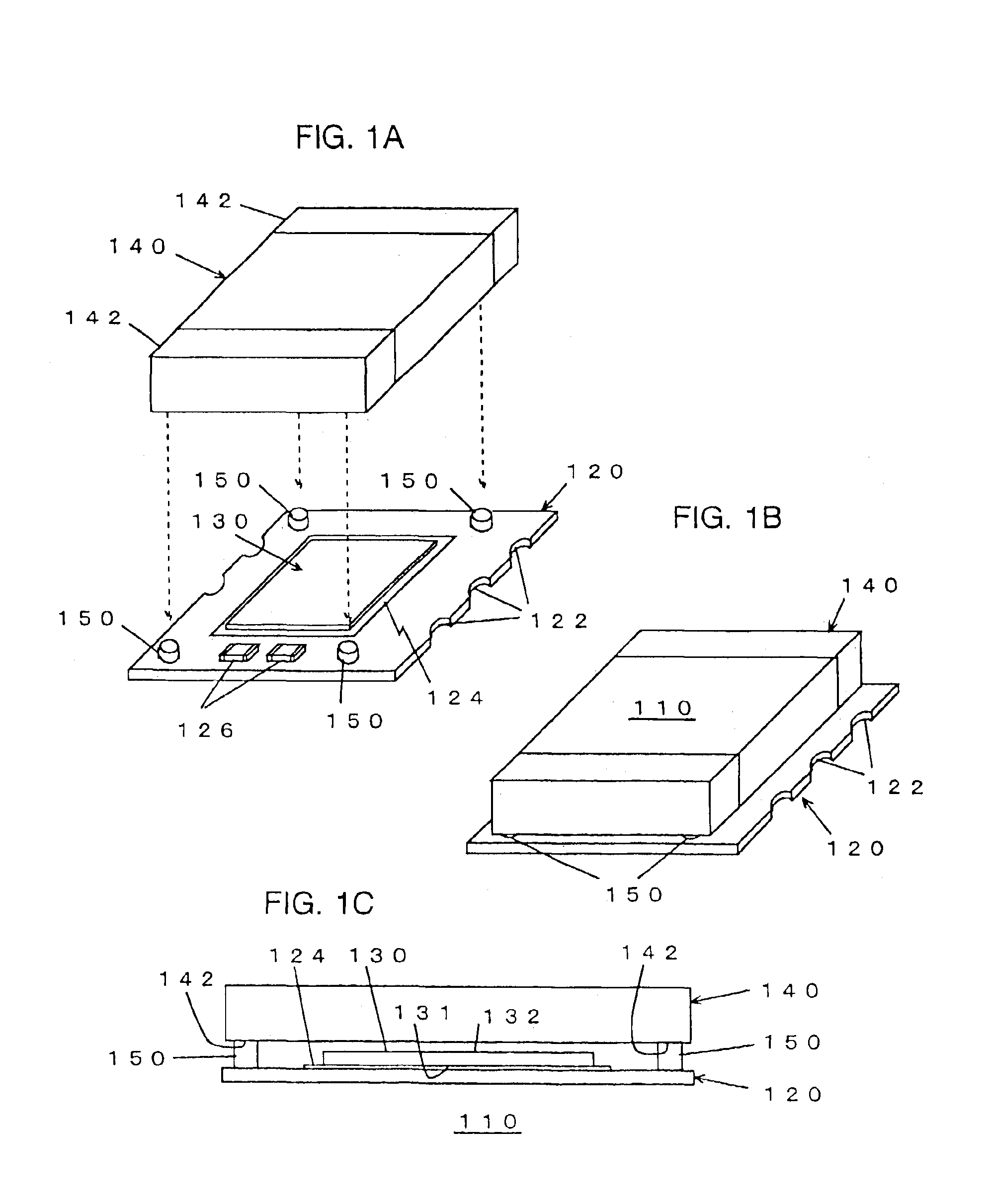
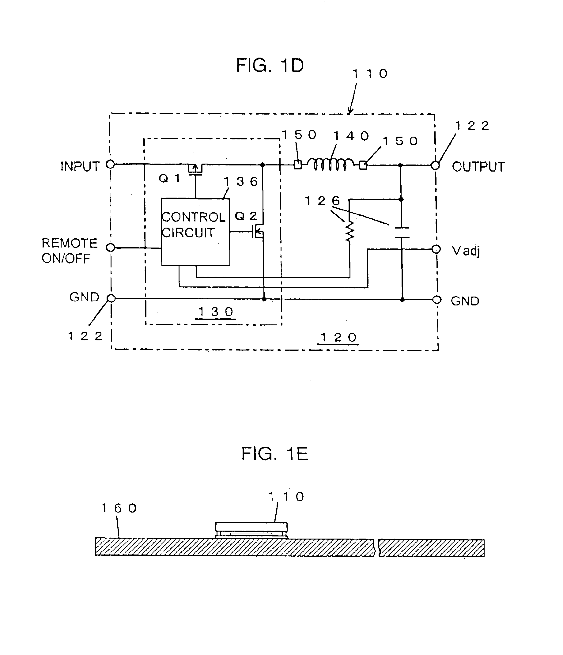
[0052]FIGS. 1A to 1D are an exploded perspective view, a perspective view, a schematic side elevation and a circuit diagram of an equivalent circuit, respectively, of a microconverter in a first embodiment according to the present invention, and FIG. 1E is a schematic sectional view of the microconverter shown in FIGS. 1A to 1D as mounted on a SM circuit board.

[0053]Referring to FIGS. 1A to 1E, a microconverter 110 is a dc-dc converter module to be surface-mounted on a SMT (Surface-Mount Technology) board 160. The microconverter 110 includes a circuit board 120, a semiconductor integrated circuit chip (hereinafter, abbreviated to “IC chip”) 130, a microinductor 140, and stud terminals 150.

[0054]The circuit board 120 is a SM circuit board and serves also as a support plate for supporting the module. The SM circuit board 120 is provided with SM electrodes and a wiring pattern on its upper surface, and side terminals 122 for surface mounting in its side surfaces. The IC chip 130, the s...

second embodiment

[0060]FIGS. 2A and 2B are a schematic side elevation and an enlarged fragmentary sectional view, respectively, of a microconverter in a second embodiment according to the present invention.

[0061]Matters relating to the second embodiment and different from those relating to the first embodiment will be described. Referring to FIGS. 2A and 2B, a microconverter in the second embodiment is provided with spherical stud terminals 150. The spherical stud terminals 150 are formed by coating resin balls 151 of a heat-resistant, elastic resin with a satisfactorily solderable (solder-wettable) metal layer 152. The spherical stud terminals 150, similarly to the aforesaid columnar stud terminals 150, are interposed between a circuit board 120 and the terminal electrodes 142 of a microinductor 140 to connect the circuit board 120 with the microinductor 140 electrically and mechanically. The spherical stud terminals 150, similarly to the columnar stud terminals 150, have a satisfactory cushioning ...

third embodiment

[0064]FIGS. 3A and 3B are a perspective view and a typical sectional view, respectively, of a microinductor 140 included in a microconverter in a third embodiment according to the present invention. FIG. 3B is an enlarged sectional view of a part A in FIG. 3A.

[0065]Referring to FIGS. 3A and 3B, each of terminal electrodes 142 of the microinductor 140 is formed by successively stacking a silver layer 143 by electroless plating, a nickel layer 144 and a tin layer 145 in that order. The top tin layer 145 is satisfactorily solderable.


PUM

PropertyMeasurementUnit
areaaaaaaaaaaa
voltageaaaaaaaaaa
heat-aaaaaaaaaa

Abstract

A surface-mount microconverter is formed by mounting a microinductor chip and a semiconductor integrated circuit chip on a circuit board. Stud terminals are arranged on the circuit board and the microinductor chip is supported on the stud terminals, and the microinductor chip and the semiconductor integrated circuit chip are superposed on the circuit board. The microconverter has an improved ability and is small and thin. The microconverter includes an effective laminated magnetic-core inductor. The inductor comprises a helical coil formed by uniting alternately superposed insulating magnetic layers and conductive pattern layers, and an annular closed magnetic path formed by the insulating magnetic layers and defining a magnetic field created by the coil. The inductor can be miniaturized in a thin chip, and a wide range in which magnetic flux density varies linearly can be secured by balancing a closed magnetic path for a magnetic field created by the coil.

Description

CROSS-REFERENCE TO RELATED APPLICATIONS[0001]The present application claims priority upon Japanese Patent Application No. 2002-218484 filed on Jul. 26, 2002, which is herein incorporated by reference.BACKGROUND OF THE INVENTION[0002]1. Field of the Invention[0003]The present invention relates to a microconverter and a laminated magnetic-core inductor. More particularly, the present invention relates to techniques effectively applicable to a microminiature dc-dc converter to be mounted on a surface-mount circuit board (SM circuit board), generally called a microconverter, and a laminated magnetic-core inductor, i.e., a principal component of the microconverter, to be used for converting a supply voltage (electromotive force) of a built-in battery included in a portable information device, such as a portable telephone, into a predetermined working voltage to be applied to a circuit.[0004]2. Description of the Related Art[0005]A portable information device, such as a portable telephone...

Claims


Application Information

Patent Timeline
Patent Type & Authority Patents(United States)
IPC IPC(8): H01F19/00H01F27/29H01F27/28H01F19/08H05K3/34H05K1/18H01L25/00H01L23/552H02M3/00H02M3/155H02M3/158
CPCH01F19/08H01F27/28H01F27/292H01L23/49811H01L23/552H01L23/645H01L25/16H02M3/00H02M3/158H05K3/3442H01L2924/13091H01L2224/16H01L2224/83102H01L2224/92125H01L2924/01025H01L2924/01078H01L2924/19104H01L2924/19105H01L2924/3025H05K1/181H05K2201/0212H05K2201/1003H05K2201/10234H05K2201/10515H05K2201/10636H05K2201/10674H01L2924/01019H01L2924/01079H05K2201/10053H01L2924/00H01L2924/00014Y02P70/50H02M3/003H01L2224/0401
Inventor NAKAO, FUMIAKIYAMASHITA, YASUOKIYOMIYA, TERUOSUZUKI, TETSUYAINAGAKI, MASAYUKIKITAOKA, MIKIO
Owner FDK CORP
Why Eureka
Try Eureka