Communications receiver with integrated IF filter and method therefor

a technology of communication receiver and filter, applied in the field of radio frequency (rf) communication receiver, can solve the problems of increasing the number of off-chip components, consuming more power, and particularly undesirable use of off-chip components, and achieve the effect of small chip die area and low power

Inactive Publication Date: 2005-04-26
NAT SCI
View PDF11 Cites 9 Cited by
  • Summary
  • Abstract
  • Description
  • Claims
  • Application Information

AI Technical Summary

Benefits of technology

[0007]It is an advantage of the present invention that an improved communications receiver having an integrated intermediate frequency (IF) filter is provided along with a method for operating a communications receiver having an integrated IF filter.
[0008]Another advantage of the present invention is that low power and a small chip die area are used by an RF receiver that has a non-tunable, on-chip IF filter.
[0009]Another advantage of the present invention is that a process-variant circuit is used to estimate an actual center frequency of a substantially non-tunable on-chip IF filter, then a tunable local oscillator is controlled so that an IF signal approximately equals the actual center frequency of the IF filter.
[0010]These and other advantages are realized in one form by an improved method of tuning an RF receiver to a desired frequency channel. The RF receiver has a common semiconductor substrate on which an intermediate frequency filter and a process-variant test circuit are formed. The method includes operating the process-variant test circuit to estimate an actual center frequency of the intermediate frequency filter. A tuning parameter is formed in response to the estimated actual center frequency and the desired frequency channel. The tuning parameter is applied to a tunable local oscillator which generates a local oscillator signal that, when mixed in a downconversion mixer with an RF signal from the desired frequency channel, generates an IF signal exhibiting approximately the actual center frequency of the IF filter.

Problems solved by technology

Traditionally, receivers have used a superheterodyne architecture that achieves acceptable results but requires a mixture of on-chip components with an excessive number of off-chip components.
The use of off-chip components is particularly undesirable for several reasons since off-chip components make such architectures larger, consume more power, less likely to maintain precise tuning, and more expensive than desired.
One particularly challenging receiver component to integrate on-chip with other components has been the IF filter.
If an IF filter exhibits a center frequency that does not closely match the fixed IF frequency, then signal-to-noise decrease and other signal deterioration effects result.
In many receiver applications, this variation in component values leads to an unacceptably imprecise IF filter center frequency, which exhibits too much variation over temperature and between different semiconductor dice, wafers, and batches.
Of course, conventional semiconductor processing techniques can also form passive analog components with lower tolerance values, but the consequences of achieving the lower tolerance values may themselves be undesirable.
However, the use of a greater die area to obtain a greater precision is undesirable because it leads to a more expensive product and otherwise consumes precious die area that may be better used for other functions.
Unfortunately, the implementation of an on-chip tunable IF filter is itself undesirable.
For example, a switched-capacitor filter design may be capable of achieving sufficient center frequency precision, but the high speed clock and switching noise which characterize this filter design make it unsuitable for many receiver applications.
Continuous time filtering (e.g., gm-C filters) may also be capable of achieving sufficient center frequency precision, but the needed precision requires complex filter-tuning circuitry which increases power consumption and uses precious semiconductor die area that can be better used for other functions.

Method used


Image

  • Communications receiver with integrated IF filter and method therefor
  • Communications receiver with integrated IF filter and method therefor
  • Communications receiver with integrated IF filter and method therefor

Examples


Embodiment Construction

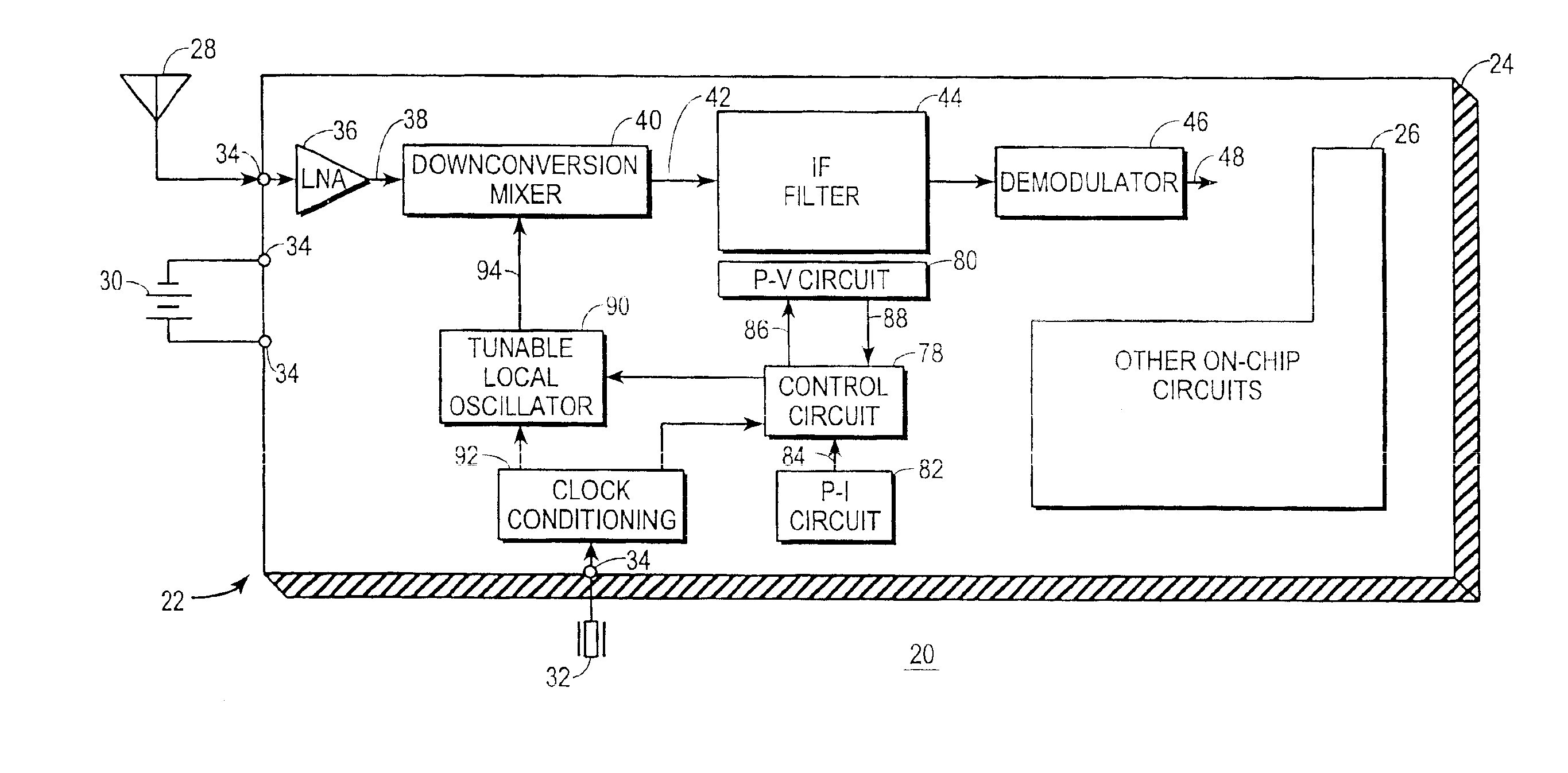
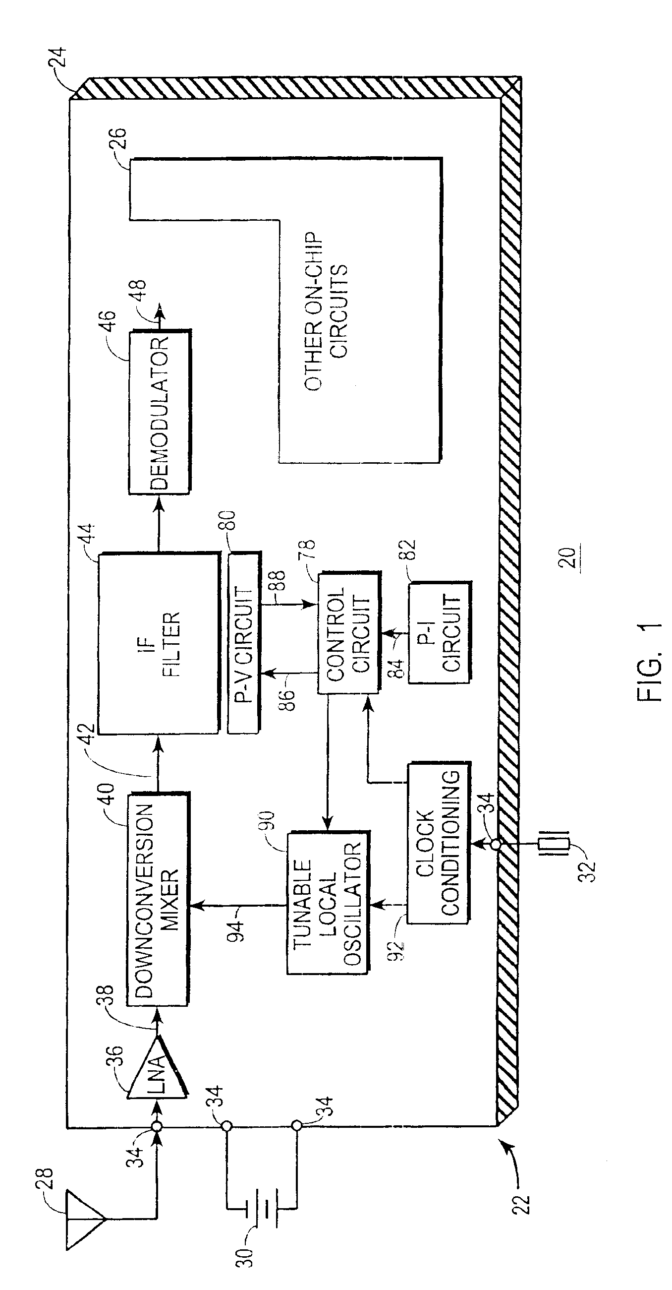
[0019]FIG. 1 shows a block diagram of a communications device 20 configured in accordance with the teaching of the present invention. Communications device 20 includes a radio-frequency (RF) receiver 22, which desirably has a highly integrated architecture with a majority of the receiver components being formed on a common semiconductor substrate 24. In addition to receiver 22, communications device 20 may include other circuits 26 formed on substrate 24. Other circuits 26 may include a modulator / transmitter, baseband processing circuits, and the like. Portable communications devices, such as wireless modems, cordless telephones, pagers, cellular telephones, radios, and the like, may benefit from communications device 20 due to its low power consumption and minimal requirements for implementation space, including semiconductor die area. However, communications device 20 is not limited to use in portable applications.

[0020]An antenna 28, a power source 30, and a crystal 32 couple to ...


PUM


Abstract

A receiver (22) includes an IF filter (44) and a nearby process-variant circuit (80) formed on a common semiconductor substrate (24). The actual center frequency of the IF filter (44) is determined by resistors (70, 74) and capacitors (72, 76) exhibiting imprecise values and is unlikely to equal a nominal center frequency. The process-variant circuit (80) includes a test resistor (102) and test capacitor (104) formed using the same resistor-forming and capacitor-forming processes used to form the IF filter resistors (70, 74) and capacitors (72, 76). In response a test signal (88) from the process-variant circuit (80) and a reference signal (84) from a process-invariant circuit (82), a tuning parameter for a tunable local oscillator (90) is determined so that a local oscillation signal (94) will exhibit a frequency which, when mixed with an RF signal (38) yields an IF signal (42) at the actual center frequency of the IF filter (44).

Description

TECHNICAL FIELD OF THE INVENTION[0001]The present invention relates generally to the field of radio-frequency (RF) communication receivers. More specifically, the present invention relates to RF receivers having on-chip intermediate frequency (IF) filters.BACKGROUND OF THE INVENTION[0002]A continuing need exists for lower power, less expensive, and physically smaller wireless devices to meet existing and future demands of portable and other electronic communications. Such demands are particularly prominent in cellular telephone, paging, wireless modem, and other applications. Traditionally, receivers have used a superheterodyne architecture that achieves acceptable results but requires a mixture of on-chip components with an excessive number of off-chip components. The use of off-chip components is particularly undesirable for several reasons since off-chip components make such architectures larger, consume more power, less likely to maintain precise tuning, and more expensive than ...

Claims


Application Information

Patent Timeline
Patent Type & Authority Patents(United States)
IPC IPC(8): H03J3/08H03J3/00
CPCH03J3/08
Inventor SEVENS, KAZIMHASHEMI, MAJID M.OZGUC, ISMAIL H.
Owner NAT SCI
Why Eureka
Try Eureka