Optimization methods for on-chip interconnect geometries suitable for ultra deep sub-micron processes

a technology of interconnection geometries and optimization methods, applied in the direction of instruments, computer aided design, basic electric elements, etc., can solve the problems of time-consuming and costly redesigns, inaccurate accuracy of models and techniques that are effective in one regime, and inability to meet the requirements of ultra deep sub-micron processes

Inactive Publication Date: 2005-05-03
CADENCE DESIGN SYST INC
View PDF13 Cites 5 Cited by
  • Summary
  • Abstract
  • Description
  • Claims
  • Application Information

AI Technical Summary

Problems solved by technology

Similarly, models and techniques that are effective in one regime begin to become unreliable when pushed into other regimes.
Although there are a number of prior art optimization methods, the accuracy of these methods has become increasingly inaccurate as technology has extended into Ultra-Deep Sub-Micron (UDSM) processing.
In deep sub-micron semiconductor process technologies, interconnect delays can easily dominate gate propagation delays as major contributors to the total delay through signal paths of an integrated circuit device.
Otherwise, unexpected timing problems in the resulting silicon may require time consuming and costly redesigns with little or no guidance on how to correct the problems.
In addition to delay, crosstalk is an issue in the design of interconnect structures for circuitry.
As a result, undesired signal coupling among interconnects is increased.
Largely, the design process has become such that integrated circuit (IC) chips cannot be designed without the help of computer-aided design (CAD) systems.

Method used


Image

  • Optimization methods for on-chip interconnect geometries suitable for ultra deep sub-micron processes
  • Optimization methods for on-chip interconnect geometries suitable for ultra deep sub-micron processes
  • Optimization methods for on-chip interconnect geometries suitable for ultra deep sub-micron processes

Examples


Embodiment Construction

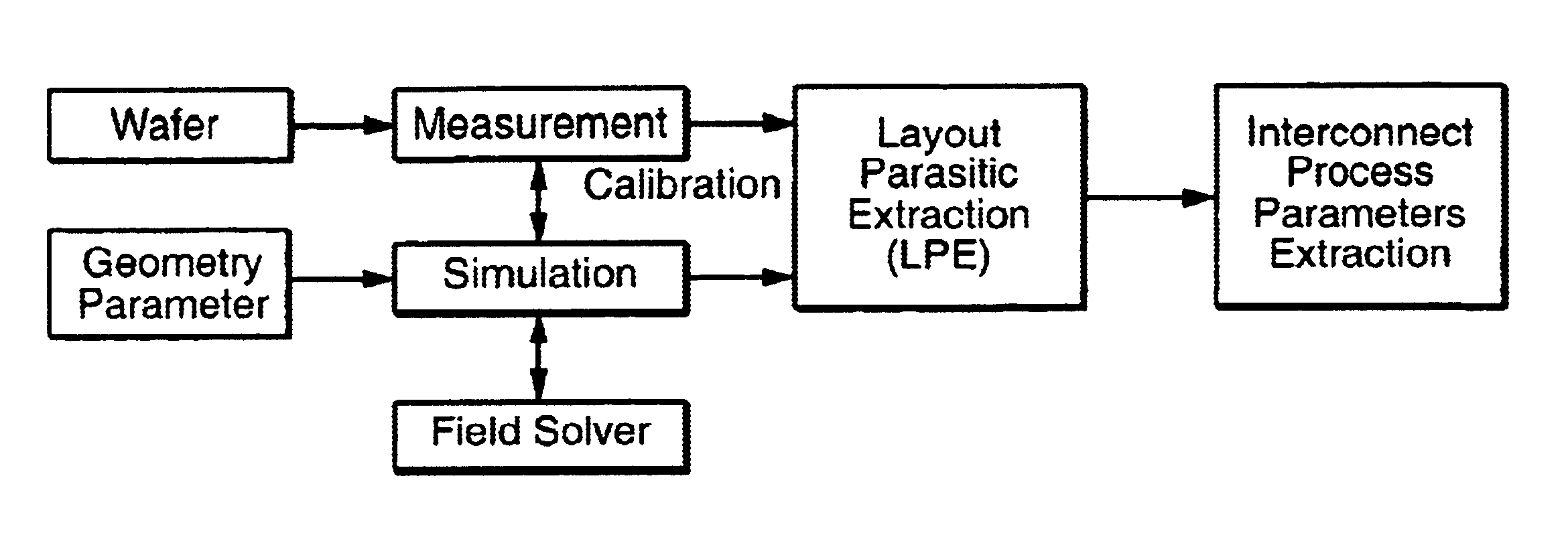
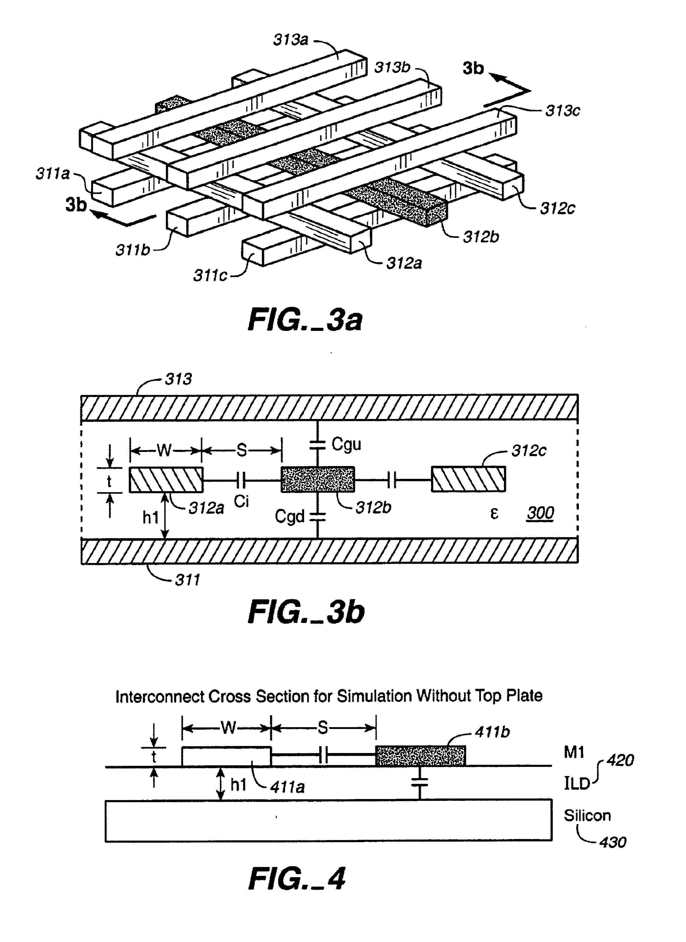
[0026]The prior art has a number of problems that lead to inaccuracies in the ultra-deep sub-micron (UDSM) region. The first of these is that the resistance and capacitance may be strongly correlated. Previous work just considers capacitance, whereas R and C are often strongly correlated in the real situations as they share common width W and length L values for the interconnect layers. When interconnect feature size is large, capacitance is dominant, but as feature size becomes smaller and smaller, the resistive part of the impedance increase and can become dominant in UDSM processes.

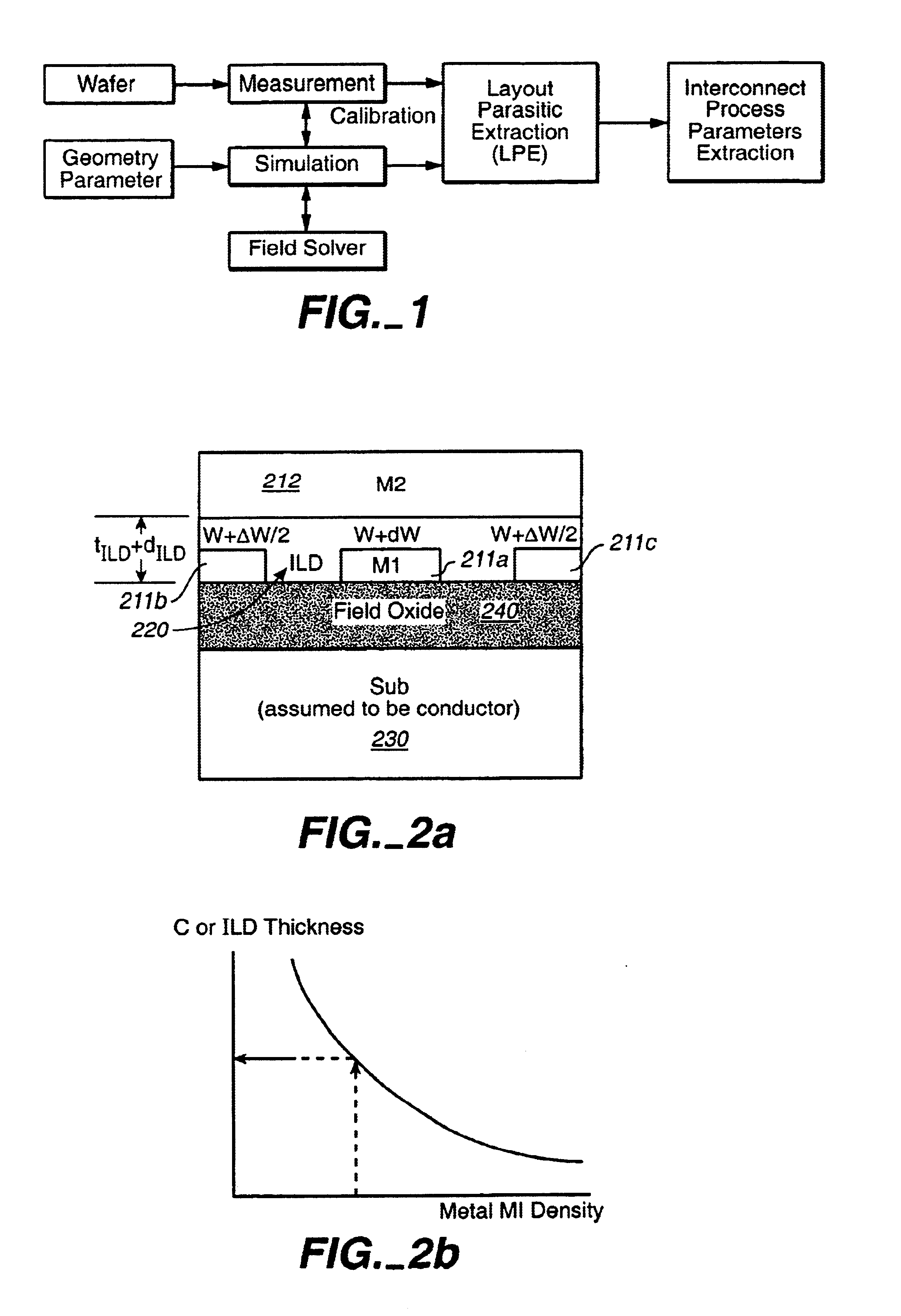
[0027]Another weakness in the prior art is that its optimized interconnect structure is incomplete. It is common in UDSM devices to use multi-dielectric and multi-conductor processes, which are not accounted for in current interconnect structures, or templates. Although in some cases these may be treated by effective values, the problem is then how to assign the effective dielectric thickness, dielectr...


PUM


Abstract

The present invention presents optimization methods for interconnect geometries that readily extend to the UDSM region for determining on-chip interconnect process parameters more realistically and accurately than in the prior art. A method for reconstruction flow that re-assembles each of a number of optimized structures into one optimized interconnect process file, such as a process technology file for extractors. This optimized process technology file can use not only extracted interconnect process parameters but also the input of LPE (Layout Parasitic Extraction) tools in physical verification stage.

Description

[0001]The present application claims priority from provisional U.S. patent application Ser. No. 60 / 387,027, filed Jun. 6, 2002.BACKGROUND OF THE INVENTION[0002]This invention pertains to the field of simulating the operation of integrated circuits, and has application to the interconnects of deep sub-micron devices.[0003]In the modeling and simulation of integrated circuits, all of the various parts need to be considered. Some of these circuit elements can be neglected in some circumstances, but begin to introduce non-negligible effects in other circumstances. Similarly, models and techniques that are effective in one regime begin to become unreliable when pushed into other regimes. In particular, one set of integrated circuit elements is the on-chip interconnect elements. Although there are a number of prior art optimization methods, the accuracy of these methods has become increasingly inaccurate as technology has extended into Ultra-Deep Sub-Micron (UDSM) processing.[0004]In deep...

Claims


Application Information

Patent Timeline
Patent Type & Authority Patents(United States)
IPC IPC(8): H01L23/522H01L21/70H01L23/52H01L21/768G06F17/50
CPCG06F17/5036H01L23/5222H01L21/76838H01L2924/3011G06F30/367H01L2924/0002H01L2924/00
Inventor JUNG, WON-YOUNG
Owner CADENCE DESIGN SYST INC
Why Eureka
Try Eureka