Modular packaging arrangements and methods

a module and packaging technology, applied in the direction of electrical apparatus construction details, electrical apparatus casings/cabinets/drawers, electrical apparatus connection, etc., can solve the problems of emi, signal integrity, electromagnetic interference (emi) and other issues that are difficult to address, and achieve the effect of maximizing board space savings

Inactive Publication Date: 2005-05-03
IBM CORP
View PDF13 Cites 13 Cited by
  • Summary
  • Abstract
  • Description
  • Claims
  • Application Information

AI Technical Summary

Benefits of technology

[0024]A further aspect of the present invention is for maximizing board space savings in addition to the other aspects.
[0025]A still further aspect of the present invention is provision for a compact product packaging that allows the formation of a wide variety of product offerings.

Problems solved by technology

Packaging and operational concerns of computer chip systems are becoming problematic given their higher operating speeds, higher power requirements as well as the ever increasing demands for their miniaturization and the additional system functionalities being added.
Consequently, electromagnetic interference (EMI) and signal integrity (SI) concerns associated with the foregoing issues are similarly difficult to address.
Moreover, further EMI and SI concerns arise given that the electronic devices in which such chip systems are used are also being driven by board level compactness considerations.
EMI is a problem because of, for example, the inductance generally associated with the relatively large area encompassed by long lead frames extending between the chip module and the surrounding passive devices on the printed circuit board.
Moreover, the printed circuit board space or real estate is consumed because these passive devices generally surround and are spaced from the chip module's periphery thereby hindering miniaturization.
While this approach has many advantages, it does not allow for customizing and modifying the components that are permanently attached to the chip.
Accordingly, known chip packaging technologies and chip-scale packaging approaches are less versatile in that they do not enable opportunities for customizing and changing components associated with a chip.
Moreover, these chip-scale packaging approaches do not allow external testing and power supply connectors to be electrically coupled to the chip modules.
Without the ability to provide semiconductor devices with enhanced power and speed functionalities especially in a compact environment so as to minimize EMI and enhance SI, the true potential of these devices is less than otherwise attainable.
Furthermore, without the ability to allow the customization or modification of such semiconductor devices in the field, their true potential is diminished.

Method used


Image

  • Modular packaging arrangements and methods
  • Modular packaging arrangements and methods
  • Modular packaging arrangements and methods

Examples


Embodiment Construction

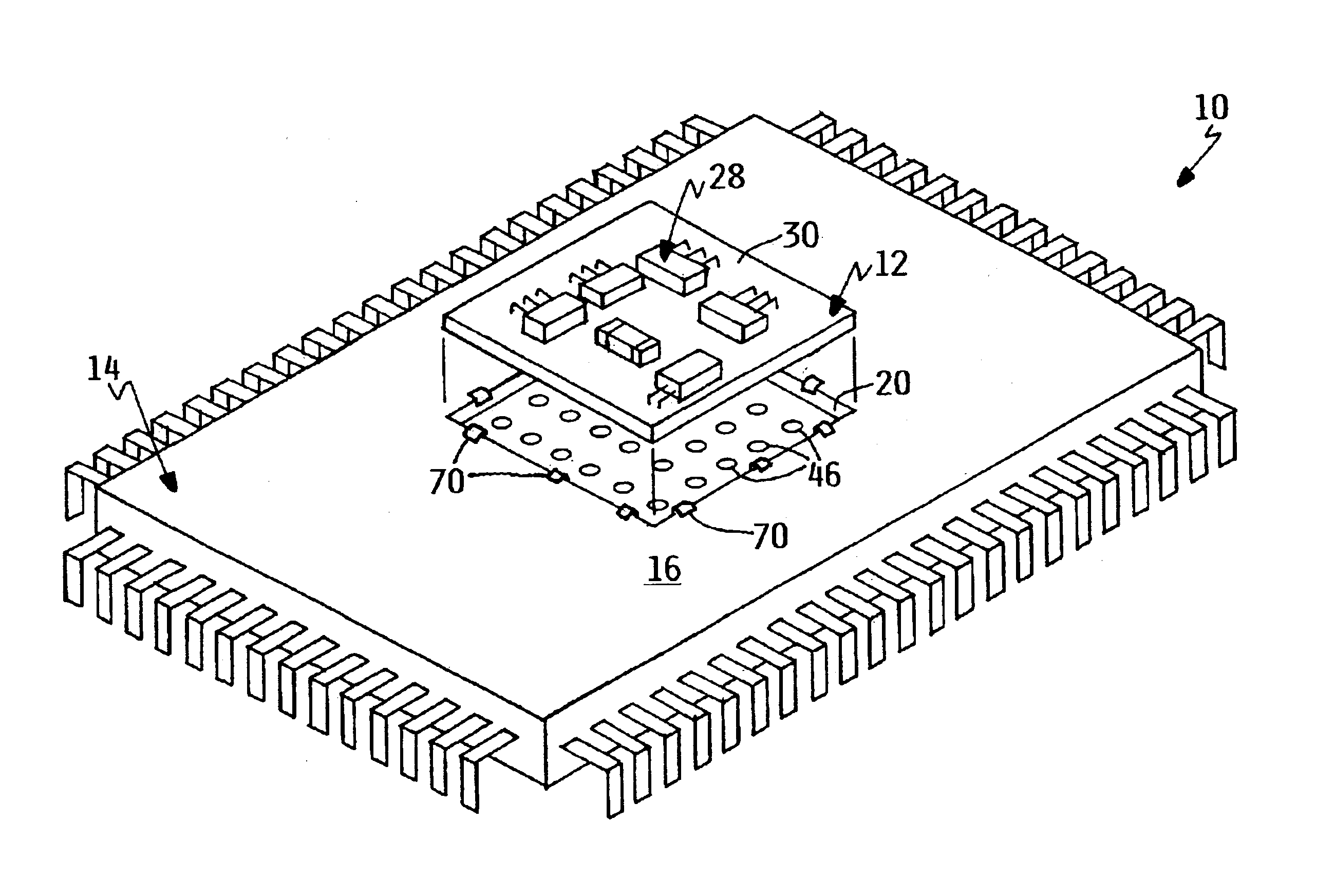
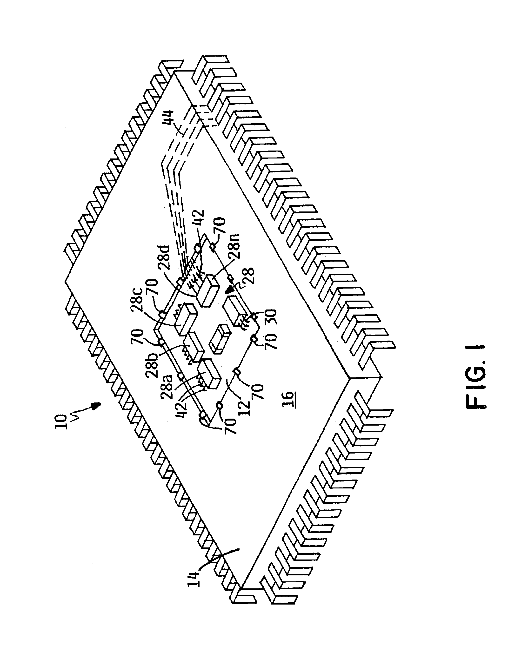
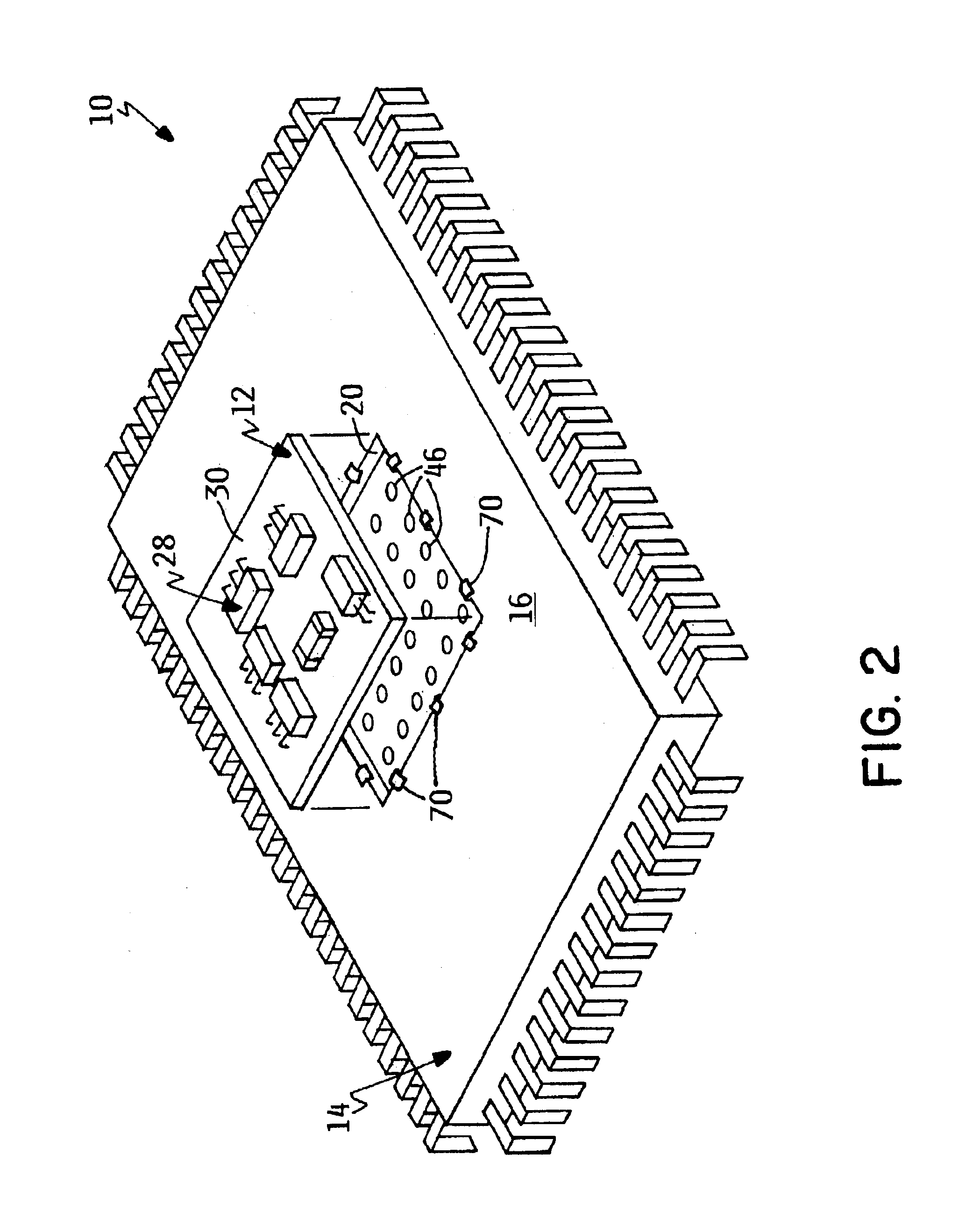
[0035]Reference is made to FIGS. 1-8 for illustrating several preferred embodiments of the present invention directed to a packaging apparatus or arrangement designated generally by reference numeral 10. In this embodiment, the packaging apparatus 10 includes a functional component assembly 12 releasably coupled to an electronic chip package or module 14 in a manner to be described.

[0036]In an exemplary preferred embodiment illustrated in FIG. 1, the functional component assembly 12 is insertable within a complementary shaped recess or socket 20 formed in a top surface 16 of a housing assembly 24 of the chip module 14. The functional component assembly 12 is positively and releasably retained by a mechanical releasable coupling assembly 26 that acts to releasably couple the functional component assembly to the housing assembly for allowing a user to customize or modify the chip module in the field. The functional component assembly need not be fitted completely in the socket 20 and ...


PUM


Abstract

The present invention relates generally to chip packaging and methods of packaging and, more particularly, to compact packaging of chips and methods thereof in electronic environments that minimize undesired electronic effects, promote speed, and enhance packaging versatility.

Description

BACKGROUND OF THE INVENTION[0001]The present invention relates generally to chip packaging and methods of packaging and, more particularly, to compact packaging of chips and methods thereof in electronic environments that minimize undesired electronic effects, promote speed, and enhance packaging versatility.[0002]Packaging and operational concerns of computer chip systems are becoming problematic given their higher operating speeds, higher power requirements as well as the ever increasing demands for their miniaturization and the additional system functionalities being added. Consequently, electromagnetic interference (EMI) and signal integrity (SI) concerns associated with the foregoing issues are similarly difficult to address. Moreover, further EMI and SI concerns arise given that the electronic devices in which such chip systems are used are also being driven by board level compactness considerations. Accordingly, achieving higher speeds, electromagnetic compatibility (EMC) and...

Claims


Application Information

Patent Timeline
Patent Type & Authority Patents(United States)
IPC IPC(8): H01L25/16
CPCH01L25/162H01L25/165H01L2924/3011H01L2224/48091H01L2924/15311H01L2224/48227H01L2924/00014H01L2924/12044H01L2924/00
Inventor GILLILAND, DON ALAN
Owner IBM CORP
Why Eureka
Try Eureka