Inexpensive wafer level MMIC chip packaging

a monolithic microwave integrated circuit and wafer level technology, applied in the direction of semiconductor devices, semiconductor/solid-state device details, electrical apparatus, etc., can solve the problems of large difference between the respective coefficients of thermal expansion (“cte”) of gaas and inp and the cte of aluminum, and the inability to direct the chip to the carrier by solder or epoxy, etc., to achieve a more reliable package

Active Publication Date: 2005-05-03
NORTHROP GRUMMAN SYST CORP
View PDF5 Cites 27 Cited by
  • Summary
  • Abstract
  • Description
  • Claims
  • Application Information

AI Technical Summary

Benefits of technology

[0009]An additional object of the invention is to protect the MMIC chip from moisture, gas or other unwanted particles without the need to hermetically seal the package.
[0010]In accordance with the foregoing objects, an inexpensive package for a semiconductor MMIC chip incorporates a stress relief buffer that absorbs thermally induced stress between the chip and the metal carrier that is produced by significantly different rates of thermal expansion of the chip and the metal carrier, providing a more reliable package. The buffer is formed by a polymer and thin metal sandwich integrally formed against the back metal on the underside of the chip, and is attached to the package carrier by solder. The polymer possesses a combination of elasticity and thermal expansion coefficient that is sufficient to provide stress relief between chip and carrier over the anticipated temperature range of operation and is capable of being chemically etched, capable of accepting a metal plating and is electrically non-conductive. Preferred polymers are polyimide and Parylene. Vias extend through the stress relief buffer to place the metal underside of the buffer and carrier layer of the package electrically in contact with the back metal layer on the back surface of the chip.

Problems solved by technology

Direct attachment of the chip to the carrier by means of solder or epoxy is impractical due to the thermo-mechanical mismatch between the GaAs or InP material of the chip and the aluminum alloy carrier.
That mismatch results from the large difference in the respective coefficients of thermal expansion (“CTE”) of both GaAs and InP with the CTE of aluminum.
That in turn produces undue levels of stress on the chip when the chip and carrier are rigidly bonded together by a bonding agent that is incapable of providing stress relief.
In that circumstance, the chip usually cracks, rendering the electronic circuits fabricated on the chip inoperative.
Solder, however, possesses a relatively high elastic modulus and low percent elongation characteristic, and, therefore, is incapable of acting as a stress buffer between the chip and the aluminum carrier during thermal expansion.
The same characteristic and inability generally exists when epoxy is used as the bonding agent.
Although epoxy has been found acceptable in some instances with some chips, the reliability as a thermal stress buffer in applicant's view has not been universally consistent.
The A40 material is expensive and brittle.
The brittleness makes the material difficult to machine to the geometry desired for the carrier.
That material is also hard and, hence, is difficult to machine.
Hermetically sealed packages require the lid to be welded to the side walls and is otherwise quite rugged, resulting in a package that is relatively heavy, housing a chip that is relatively light in weight, a package that weighs considerably more than one that is not hermetically sealed.

Method used


Image

  • Inexpensive wafer level MMIC chip packaging
  • Inexpensive wafer level MMIC chip packaging

Examples


Embodiment Construction

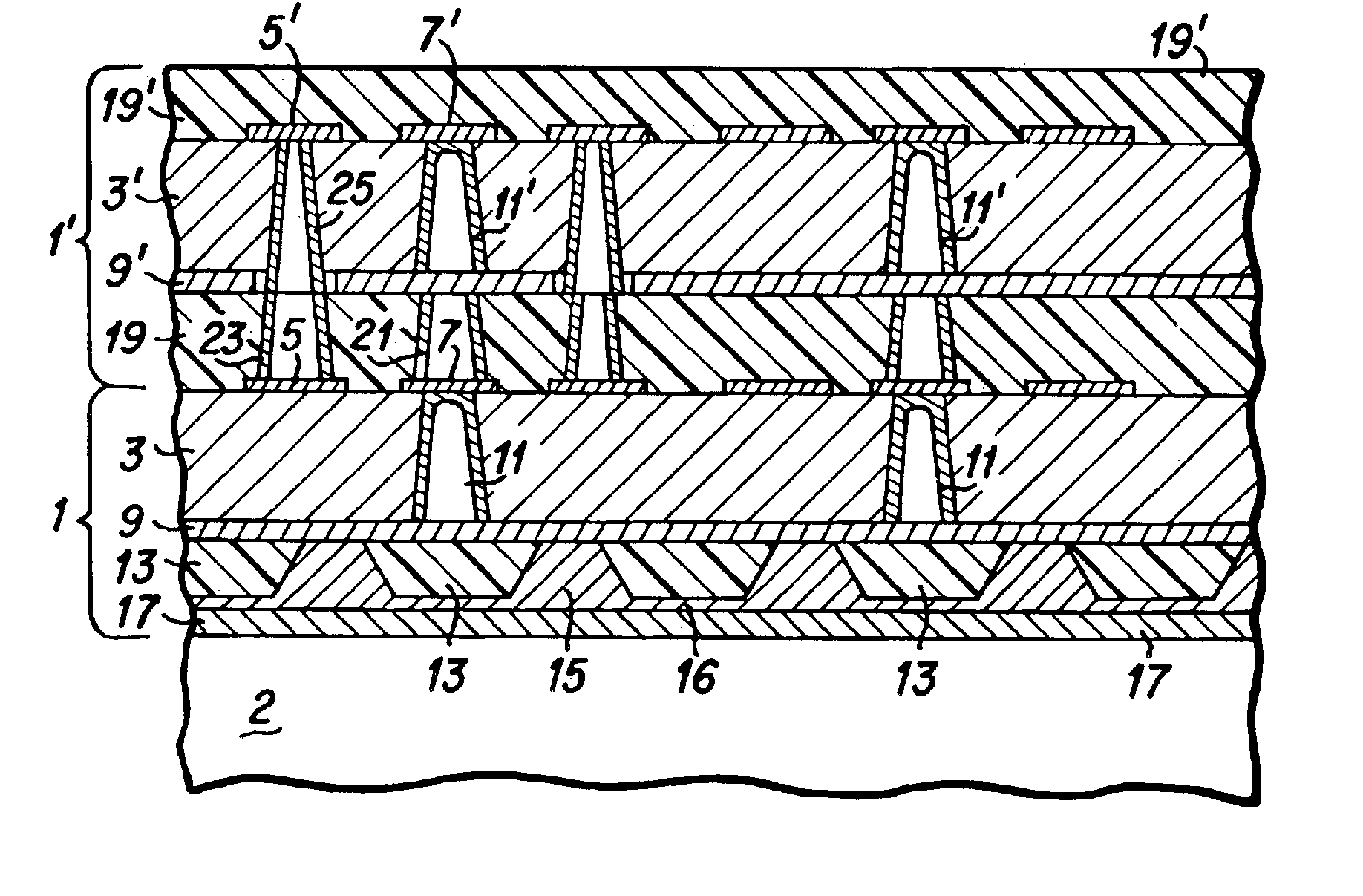
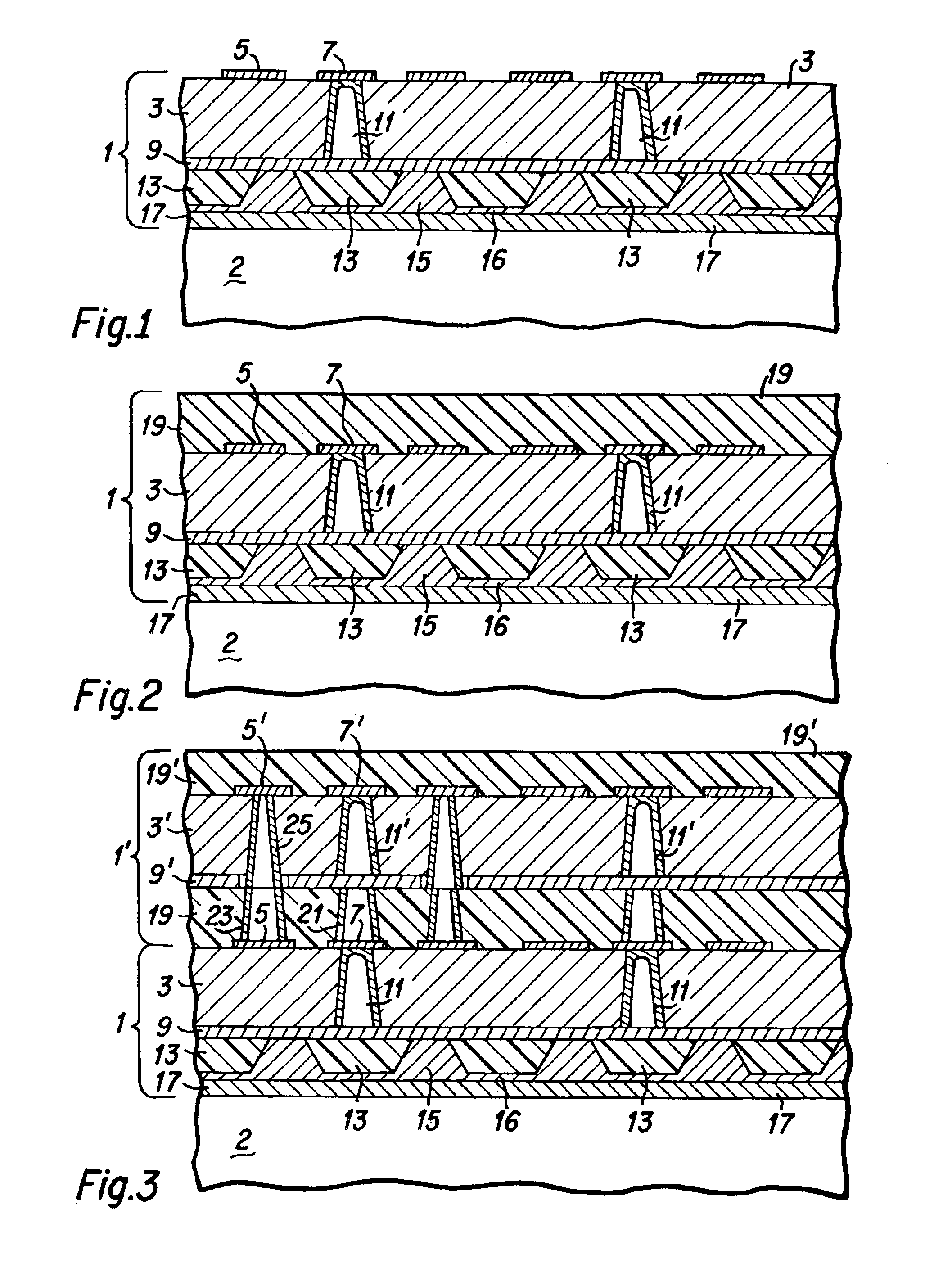
[0017]MMIC chips intended for multi-chip modules (“MCMs”) are formed in and detached from wafers of semiconductor material using known processes, the details of which are not material to or necessary for an understanding of the present invention. The multi-chip module contains two or more of such MMIC chips that are positioned in respective compartments of the module as prescribed by the designer. Those MMIC chips are typically connected in circuit and function together to accomplish whatever the functions intended by the designer of the MCM. The functional electronic devices, integrated circuit semiconductor devices, formed in and / or on the chip are accessible on upper surface of the chip. Essentially the MCM serves as the package for the MMIC chip. A thin metal layer, referred to as the ground plane layer or as the back metal, is formed on and covers the flat bottom surface of the chip. That back metal is the surface that attaches to the metal carrier, which serves as a floor of t...


PUM


Abstract

An inexpensive package for a semiconductor chip (1) that incorporates a stress relief buffer (13) between a side of the chip and the metal carrier layer (2) to absorb thermally induced stress produced by significantly different rates of thermal expansion of the wafer and the metal carrier. The buffer (13) is formed by a polymer that is flexible and can be etched, contains a coefficient of thermal expansion that does not significantly differ from that of the chip and/or a combination of CET and elasticity that retains a physical connection with the side of the chip and the metal carrier over the temperature range of operation anticipated for the chip. Polyimide or paraylene are preferred examples. Vias (15) extend through the buffer to place the metal carrier electrically in common with the metal layer (5) found on the back surface of the wafer so that an electrical ground applied to the metal carrier layer (2) may extend through to that surface.

Description

FIELD OF THE INVENTION[0001]This invention relates to packaging of semiconductor chips, and, more particularly, to a new and inexpensive technique for the packaging of monolithic microwave integrated circuit chips that minimizes thermally induced mechanical stresses and to the packaged chip assembly resulting therefrom.BACKGROUND[0002]By definition a monolithic microwave integrated circuit (“MMIC”) device contains all of the active and passive circuit elements and associated interconnections formed either in site on or within a semi-insulating substrate, such as a semiconductor, or insulating substrate by one or more well known deposition processes. Typically the MMIC device is formed on a semiconductor chip (or group of semiconductor chips) and the chip is (or chips are) assembled into a package.[0003]A first step in the packaging of a semiconductor chip for a MMIC circuit application is to attach the chip to a metal carrier, suitably a carrier of conventional aluminum alloys, whic...

Claims


Application Information

Patent Timeline
Patent Type & Authority Patents(United States)
IPC IPC(8): H01L23/373H01L23/488H01L23/58H01L23/48H01L23/34H01L23/66
CPCH01L23/3735H01L23/481H01L23/488H01L23/66H01L2924/0002H01L2924/00
Inventor ROGERS, HARVEY NEWELLKINTIS, MARK
Owner NORTHROP GRUMMAN SYST CORP
Why Eureka
Try Eureka