Semiconductor memory device and erase method for memory array

a memory array and memory technology, applied in semiconductor devices, digital storage, instruments, etc., can solve the problems of deterioration of reliability, source voltage cannot be increased higher, erase speed cannot be enhanced, etc., and achieve the effect of reducing non-uniformity

Active Publication Date: 2005-05-03
SHARP KK
View PDF3 Cites 156 Cited by
  • Summary
  • Abstract
  • Description
  • Claims
  • Application Information

AI Technical Summary

Benefits of technology

[0028]Preferably, in the individual-erase mode, for an erase-target memory cell in the memory cells in the memory cell array, the erase method performs operation such that after voltage application is performed under the application condition of the individual-erase mode, a determination is performed whether the memory cell has been erased; for the memory cell erased, the operation terminates the voltage application in progress under th...

Problems solved by technology

However, when the source voltage is increased, inter-band tunneling current is also increased, so that holes are trapped into the tunnel oxide layer, thereby leading to deterioration of reliability.
For this reason, the source voltage cannot be increased higher than a given level, and hence the erase speed also cannot b...

Method used


Image

  • Semiconductor memory device and erase method for memory array
  • Semiconductor memory device and erase method for memory array
  • Semiconductor memory device and erase method for memory array

Examples


Embodiment Construction

[0041]Embodiments of a semiconductor memory device and an erase method for a memory cell array according to the present invention will be described with reference to the accompanying drawings.

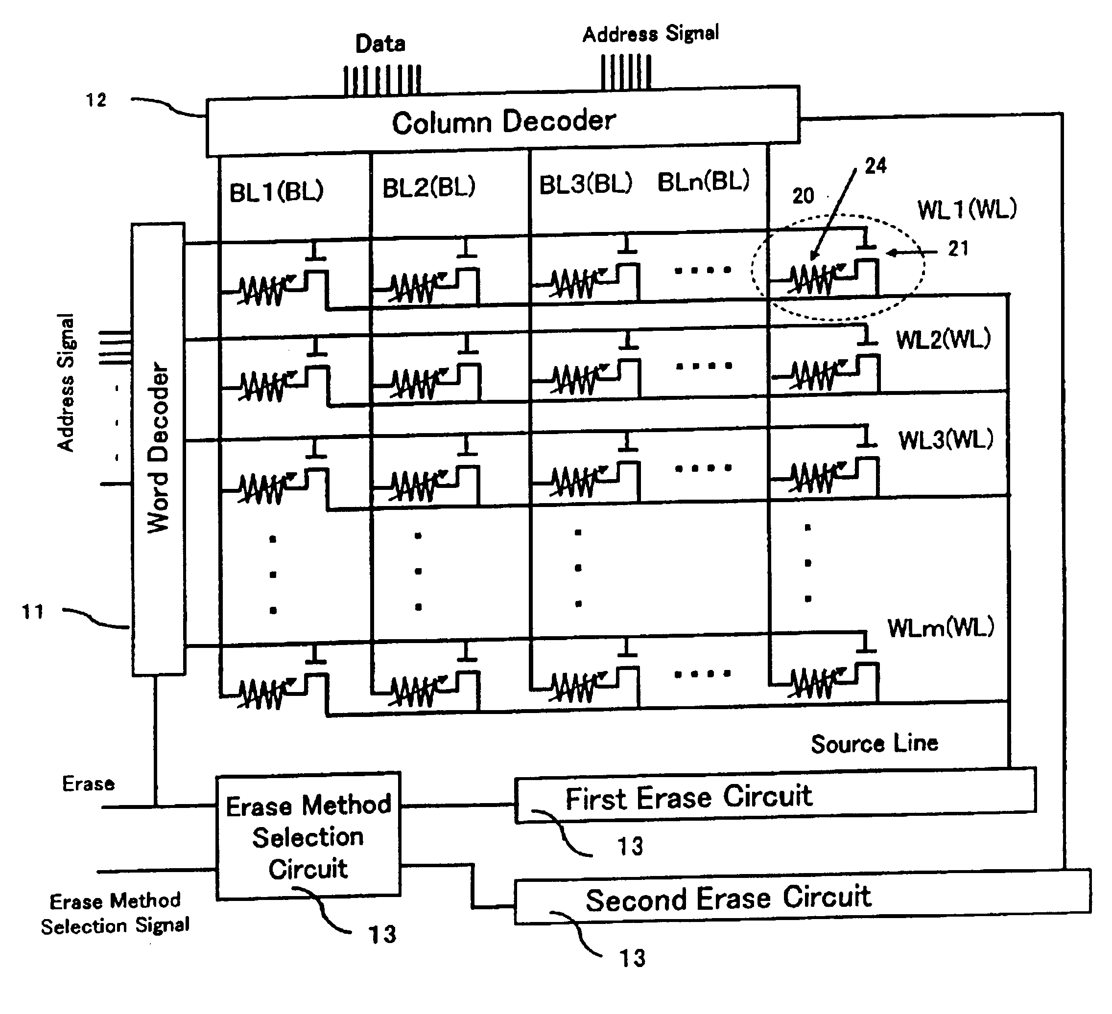
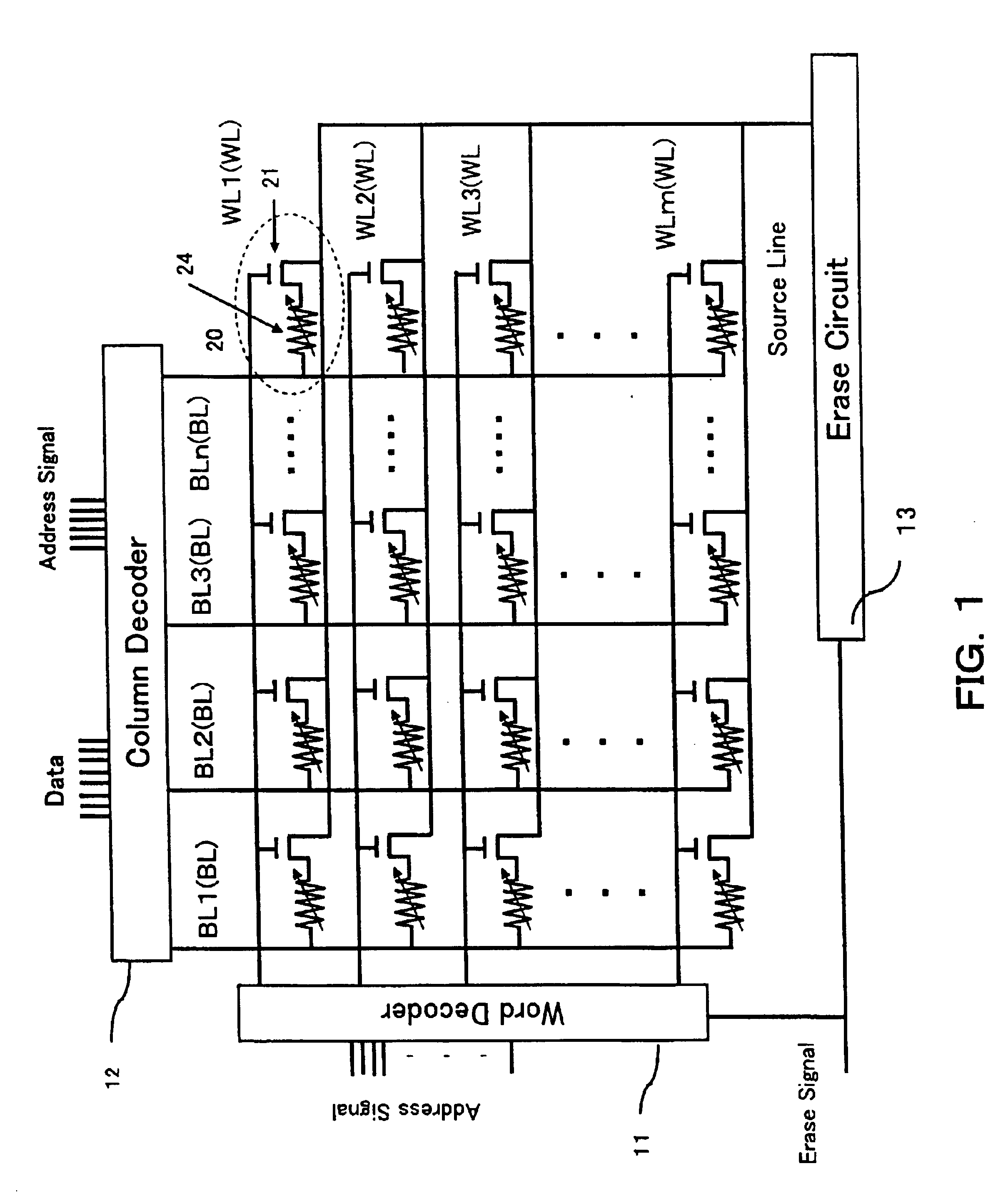
[0042]Referring to FIG. 1, the semiconductor memory device of the present invention has a single or a plurality of memory cell arrays each configured as described hereunder. A plurality of nonvolatile memory cells 20 are arranged in each of a row direction and column direction, and a plurality of word lines WL1, . . . , WLm and a plurality of bit lines BL1, . . . , BLn are arranged in each of the row direction and column direction to select a predetermined memory cell or predetermined memory cells from the plurality of memory cells 20.

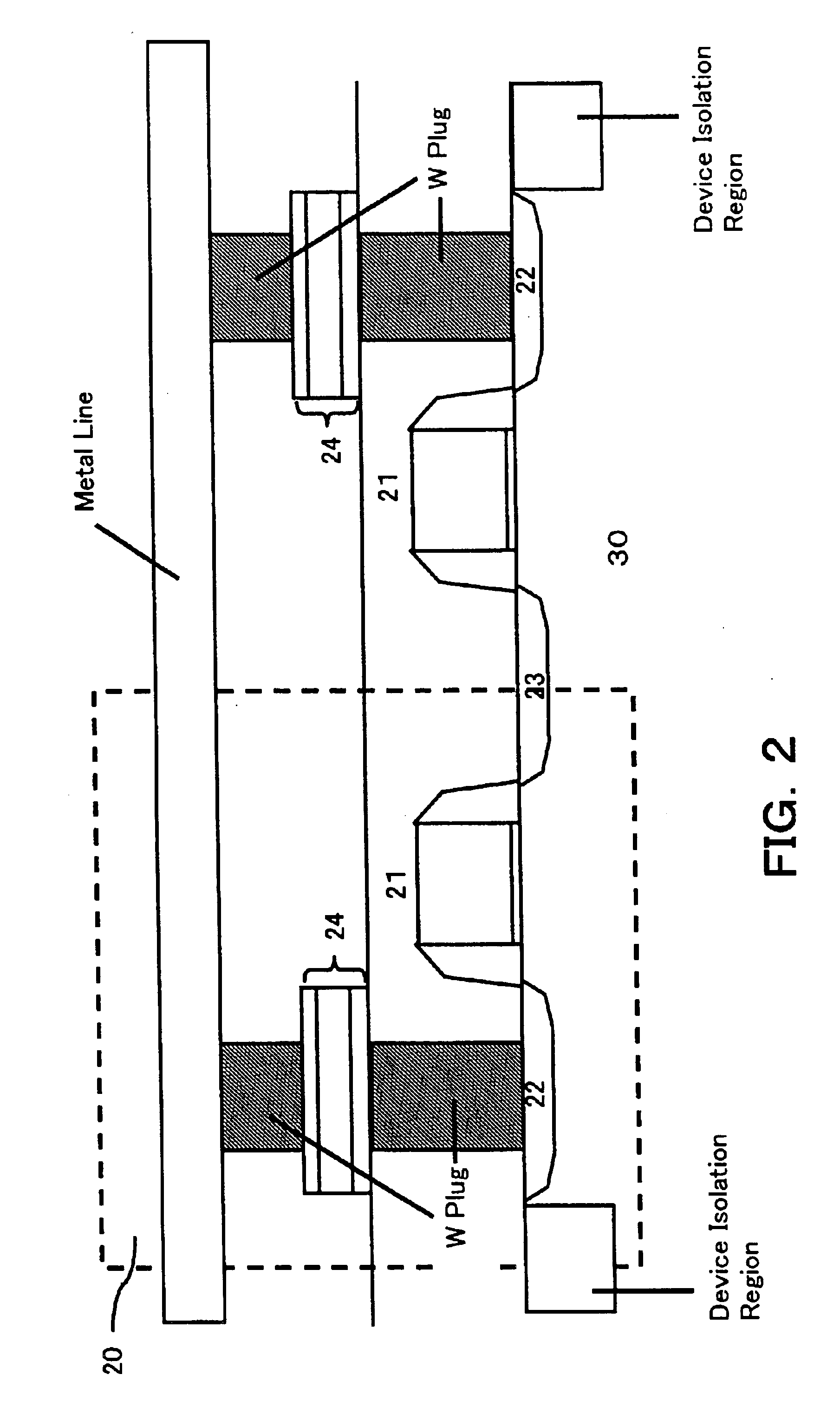
[0043]The memory cells 20 are arranged as follows. One end sides of variable resistor elements 24 for storing information by using variations in electric resistance are connected to drains of selection transistors 21. In the memory cell array, the other end sides ...


PUM


Abstract

An object of the invention is to provide a nonvolatile semiconductor memory device and an erase method for a memory cell array that have high degree of freedom and that are capable of quickly and securely implementing data erase and reprogramming. In a memory cell array, memory cells each configured of a variable resistor element for storing information through variations in electric resistance and a selected transistor are arranged in a matrix, and word lines (WL1, . . . , WLm) and bit lines (BL1, . . . , BLn) are arranged to select a predetermined memory cell. For the memory cell array, erase means is provided that sets the electric resistance of the variable resistor element to a predetermined erased state by applying voltage under a predetermined application condition to the word line (WL), bit line (BL), and source line (SL). The erase means switches between a batch-erase mode and an individual-erase mode. The batch-erase mode is used to perform batch erase of all the memory cells in the memory cell array, and the individual-erase mode is used to perform individual erase of a part of the memory cells in the memory cell array.

Description

BACKGROUND OF THE INVENTION[0001]1. Field of the Invention[0002]The present invention relates to a semiconductor memory device that has a single or a plurality of memory cell arrays each configured such that a plurality of nonvolatile memory cells are arranged in each of a row direction and column direction, and a plurality of word lines and a plurality of bit lines are arranged in each of the row direction and column direction to select a predetermined memory cell or predetermined memory cells from the plurality of memory cells. More specifically, the present invention relates to an erase method for a memory cell array using variable resistor elements as memory bearers.[0003]2. Description of the Related Art[0004]Recent semiconductor memory devices are in a fast-growing field. Especially, flash memories can be electrically reprogrammed, and data once programmed therein are not erased even after power-off. Because of these features, flash memories are used with easy-to-carry memory ...

Claims


Application Information

Patent Timeline
IPC IPC(8): G11C16/16G11C16/02G11C13/00G11C16/06G11C11/15G11C11/16G11C11/56H01L21/8246H01L27/10H01L27/105
CPCG11C11/5678G11C11/5685G11C13/0007G11C13/0069G11C13/0097G11C13/0064G11C11/16G11C13/0004G11C2213/79G11C2013/009G11C2213/31G11C11/15
Inventor MORIMOTO, HIDENORI
Owner SHARP KK
Why Eureka
Try Eureka