Pixel structure and an associated method of fabricating the same

a bolometer and focal plane array technology, applied in the field of infrared detectors, can solve the problems of limiting the length of the legs, consuming significant amounts of energy, and generally uncooled, and achieve the optimal performance of the pixel structure, maximize the area of the detector and the insulator, and maximize the absorption characteristics of the bolometer

Inactive Publication Date: 2005-05-10
DRS NETWORK & IMAGING SYST
View PDF13 Cites 6 Cited by
  • Summary
  • Abstract
  • Description
  • Claims
  • Application Information

AI Technical Summary

Benefits of technology

[0015]In light of the foregoing background, the present invention provides a pixel structure which typically forms one element of a focal plane array and which includes a bolometer having a detector and an insulator (e.g., thermal isolation structure) in a spaced apart relationship. The insulator includes a plurality of legs where, in one embodiment, the legs are disposed underneath the detector, so as to maximize the area of the detector and the length of the legs of the insulator and, thus, optimize the performance of the pixel structure. In this regard, maximizing the area of the detector increases the absorption efficiency of the bolometer and reduces the level of 1 / f noise. Additionally, by increasing the length of the legs, such as by including serpentine legs in one embodiment, the absorption efficiency is increased, the thermal resistance of the bolometer is increased, and the thermal loss to the substrate is minimized.
[0016]In addition, the bolometer includes a resonant layer that, along with the detector and insulator, forms two resonant absorption cavities to increase the absorption efficiency of the bolometer. In this regard, the resonant layer is selected such that it is impedance matched with vacuum so that the emissivity of the bolometer approaches unity. Also, a method is provided for fabricating a pixel structure of a bolometer-based focal plane array in which the insulator is disposed underneath the detector so as to likewise facilitate maximizing the area of the detector and insulator.
[0020]Since the bolometer of one advantageous embodiment has an insulator with serpentine legs disposed underneath the detector, the area of the detector and the length of the legs can be maximized so as to optimize the performance of the pixel structure. For example, in order to increase the absorption characteristics of the pixel structure, the detector, which absorbs the incident thermal radiation, is preferably relatively large. By filling most, if not all, of the footprint of the pixel structure with the respective detector, the focal plane array of the present invention maximizes the fill factor. In addition, maximizing the area of the detector with respect to the footprint size of the pixel structure minimizes the level of 1 / f noise since the area of the detector and level of noise are inversely proportional.
[0021]By placing the insulator between the substrate and detector and disposing the legs of the insulator underneath the detector according to one advantageous embodiment, thermal loss to the substrate can also be minimized. As previously mentioned, conventional bolometers generally include two or more legs that extend between the bolometer and the substrate and support the bolometer above the substrate and help reduce thermal loss to the substrate. Because, the legs of conventional bolometers typically extend out from edge portions of the absorber and transducer, the length of the legs are limited, which limits the thermal isolation of the bolometer. In contrast, by permitting the detector to overlie the insulating legs and / or by forming the insulating legs in a two-dimensional serpentine shape, the bolometer of the present invention can maximize the length of the legs of the insulator. Maximizing the length of the legs maximizes the thermal isolation of the detector with respect to the substrate which, combined with the absorption efficiency of the detector, increases the sensitivity and, thus, thermal resistance, of the bolometer.
[0026]By preferably disposing the insulator underneath the detector in the bolometer of the present invention, the area of the detector and insulator can be maximized, which allows for optimal performance of the pixel structure. As such, the absorption characteristics of the bolometer can be maximized, and 1 / f noise can be minimized. Additionally, the thermal loss of the bolometer to the substrate can be reduced due to increases in the length of the insulator legs which, combined with the increased absorption characteristics, increases the thermal resistance of the bolometer. Moreover, by including the resonant layer, the absorption efficiency of the bolometer is greatly increased over conventional systems.

Problems solved by technology

As a result, quantum detectors that operate at cryogenic temperatures can have a relatively complex design and generally consume significant amounts of energy.
Thermal detectors are typically uncooled and therefore generally operate at room temperature.
This is a drawback in conventional bolometers because for a given pixel structure size, the available area must be divided between the TIS, and the absorber and transducer, which limits the length of the legs and, in turn, the thermal isolation of the bolometer.
Most notably, for the bolometer of each pixel structure, the characteristics of the absorber element and the transducer element cannot be separately optimized since the absorber and transducer elements are included within the same multilayer structure that is supported above the surface of the substrate.
Unfortunately, the legs, pillars or the like that support the absorber and transducer elements of conventional bolometers above the surface of the substrate generally extend from edge portions of the absorber and transducer elements to the substrate.
Due to the design of these conventional bolometers, the absorber layer is therefore typically unable to completely cover the legs, pillars or the like.
While conventional focal plane arrays having pixel structures with bolometers as described above have been sufficient for most applications in the past, these conventional focal plane arrays may be unable to meet the heightened requirements proposed by a number of future applications that demand increased performance and perhaps decreased size.
In particular, as the pixel density and performance requirements of focal plane arrays are increased, the compromises that have been made in the past in order to balance the absorption characteristics of a conventional bolometer become unworkable.
For the reasons described above, conventional focal plane arrays having a plurality of pixel structures, each of which includes a bolometer having absorber and transducer supported above the surface of a substrate, do not appear to be able to meet the performance requirements demanded by some modern applications.
In this regard, certain types of materials used to create the transducer element of many bolometers generally cause some level of a low frequency, 1 / f, noise in the signal generated by passing current through the transducer element.
Therefore, smaller area transducers tend to exhibit higher levels of 1 / f noise than do larger area transducers.
This 1 / f noise is a drawback to the focal plane array because 1 / f noise generally limits the ability of the infrared detector to effectively calibrate for other types of noise, such as spatial pattern noise, thereby removing these other types of noise from the signal generated by passing current through the transducer element.

Method used


Image

  • Pixel structure and an associated method of fabricating the same
  • Pixel structure and an associated method of fabricating the same
  • Pixel structure and an associated method of fabricating the same

Examples


Embodiment Construction

[0035]The present invention now will be described more fully hereinafter with reference to the accompanying drawings, in which preferred embodiments of the invention are shown. This invention may, however, be embodied in many different forms and should not be construed as limited to the embodiments set forth herein; rather, these embodiments are provided so that this disclosure will be thorough and complete, and will fully convey the scope of the invention to those skilled in the art. Like numbers refer to like elements throughout.

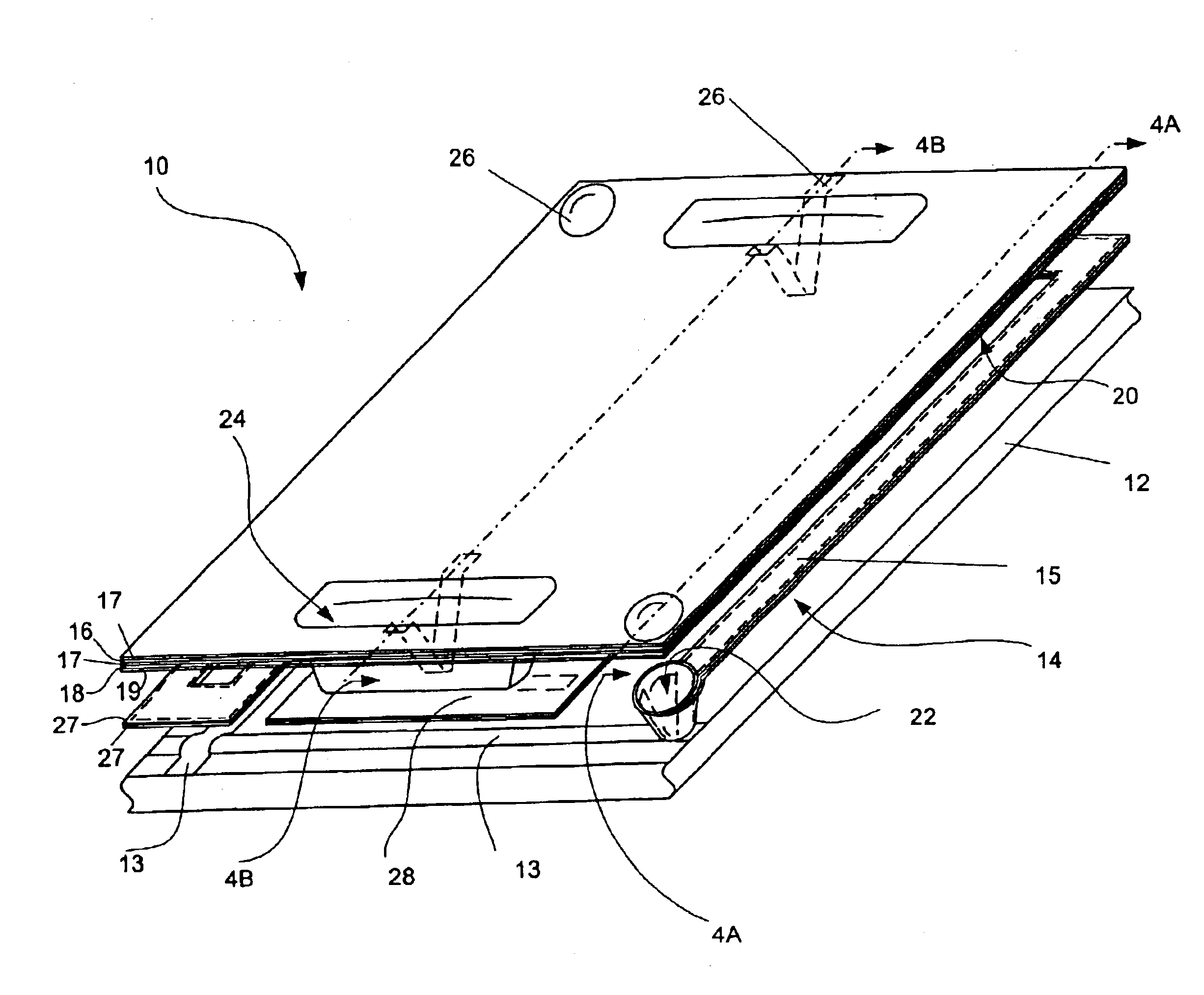
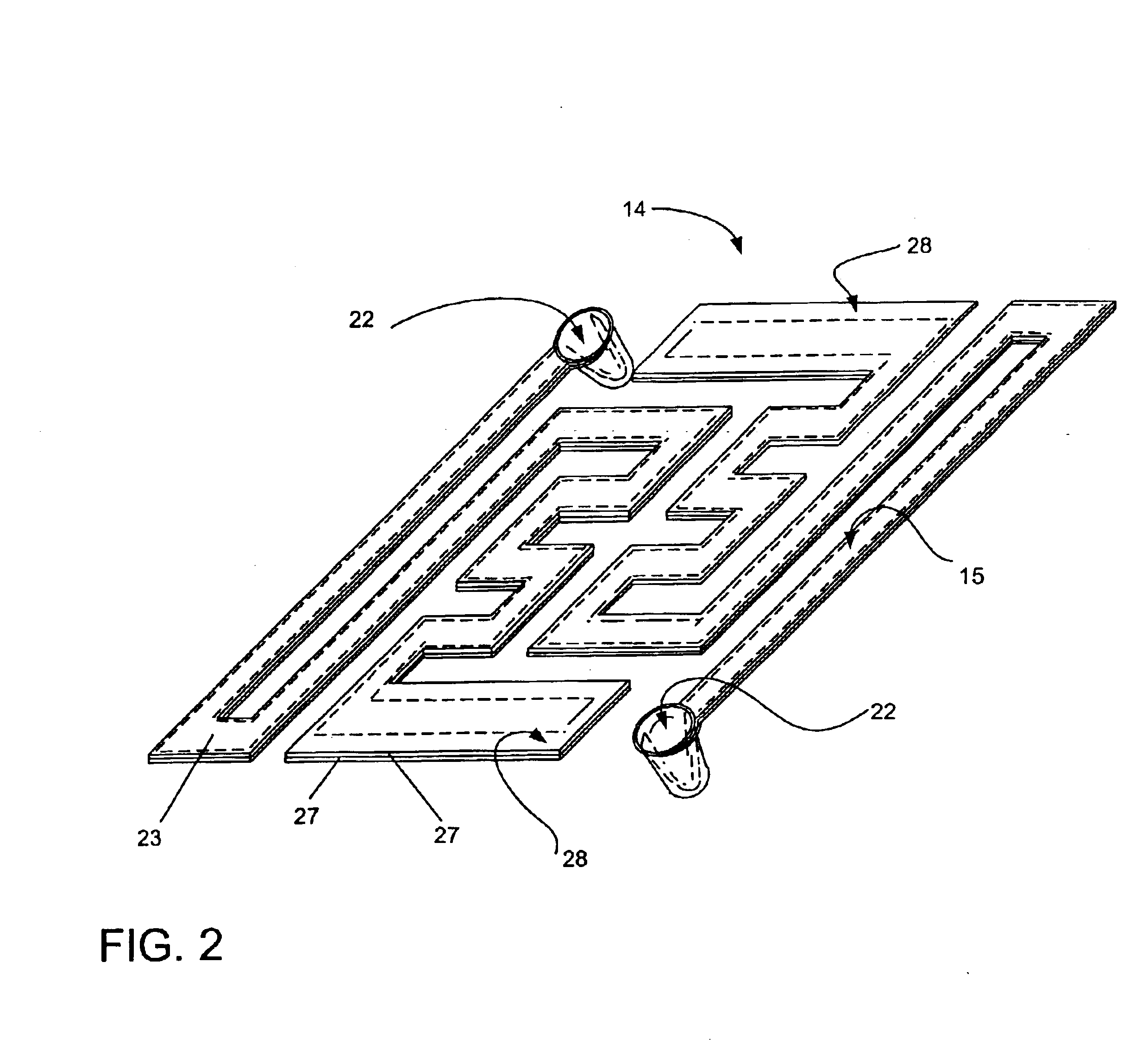
[0036]Referring now to FIG. 1, a pixel structure 10 according to one advantageous embodiment of the present invention is illustrated. As shown, the pixel structure includes a substrate 12 and a bolometer disposed upon the substrate. As known to those skilled in the art, a focal plane array typically includes an array of pixel structures, thereby forming an uncooled infrared focal plane array. Although the array can have different sizes, such as 320 rows by...


PUM


Abstract

A pixel structure, which forms one element of a focal plane array, includes a bolometer having a detector and an insulator. The detector that is made from a material that absorbs incident thermal radiation and has an electrical resistance that varies in response to changes in the temperature of the material. The insulator has a plurality of serpentine legs disposed completely underneath the detector so that the insulator extends between the detector and the substrate. And the insulator supports the detector in a spaced-apart relationship with respect to the substrate to thermally isolate the detector from the substrate. To further improve the performance of the bolometer, the bolometer includes a resonant layer between the detector and the insulator. The resonant layer is disposed such that areas defined between the detector and the resonant layer, and between the resonant layer and the insulator, form first and second resonant cavities, respectively.

Description

FIELD OF THE INVENTION[0001]The present invention relates generally to infrared detectors and methods of fabricating the same and, more particularly, to the pixel structure of a bolometer-based focal plane array and methods of fabricating the same.BACKGROUND OF THE INVENTION[0002]Infrared detectors are used in a variety of applications to provide an electrical output which is a useful measure of the incident infrared radiation. For example, quantum detectors are one type of infrared detector that are often used for night vision purposes in a variety of military, industrial and commercial applications. Quantum detectors generally operate at cryogenic temperatures and therefore require a cryogenic cooling apparatus. As a result, quantum detectors that operate at cryogenic temperatures can have a relatively complex design and generally consume significant amounts of energy.[0003]Another type of infrared detector is a thermal detector. Thermal detectors are typically uncooled and theref...

Claims


Application Information

Patent Timeline
Patent Type & Authority Patents(United States)
IPC IPC(8): G01J5/00G09G1/00H01L31/02G01J5/20G09GH01L27/146
CPCH01L27/14669G01J5/20
Inventor IONESCU, ADRIAN C.HOWARD, PHILIP EARL
Owner DRS NETWORK & IMAGING SYST
Why Eureka
Try Eureka