Application-specific testing methods for programmable logic devices

a programmable logic and application-specific testing technology, applied in the field of programmable logic devices, can solve the problems of increasing the cost of already expensive plds, reducing the probability of finding defects on a given chip, and achieving the effect of avoiding defects

Inactive Publication Date: 2005-05-10
XILINX INC
View PDF24 Cites 43 Cited by
  • Summary
  • Abstract
  • Description
  • Claims
  • Application Information

AI Technical Summary

Benefits of technology

[0008]The present invention enables PLD manufactures to identify PLDs that, despite some defects, can flawlessly implement selected customer designs.

Problems solved by technology

Unfortunately, as chip size increases, so too does the probability of finding a defect on a given chip.
The process yield therefore decreases with PLD complexity, making already expensive PLDs still more expensive.
Not knowing in advance the purpose to which a given PLD will be dedicated places a heavy burden on the quality and reliability of the PLD because PLD vendors must verify the functionality of any feature that might be used.
It has been found that, for some large chips, close to two thirds of the chips on a given wafer may be discarded because of localized defects.
Considering the costs associated with manufacturing large integrated circuits, discarding a large percentage of PLD chips has very significant adverse economic impact on PLD manufacturers.
Subsequent to fabrication, the various chips on a given semiconductor wafer are tested for “gross” defects, such as power-supply shorts, that have a high probability of rendering a PLD unfit for any customer purpose.
The foregoing test methods will not forestall PLD vendors from selling fully tested, defect-free PLDs.

Method used


Image

  • Application-specific testing methods for programmable logic devices
  • Application-specific testing methods for programmable logic devices
  • Application-specific testing methods for programmable logic devices

Examples


Embodiment Construction

[0037]The present invention relates to programmable logic devices. In the following description, numerous specific details are set forth to provide a more thorough understanding of embodiments of the present invention. However, it will be apparent to one skilled in the art that the present invention may be practiced without these specific details. In other instances, well-known features have not been described in detail in order to avoid obscuring the present invention.

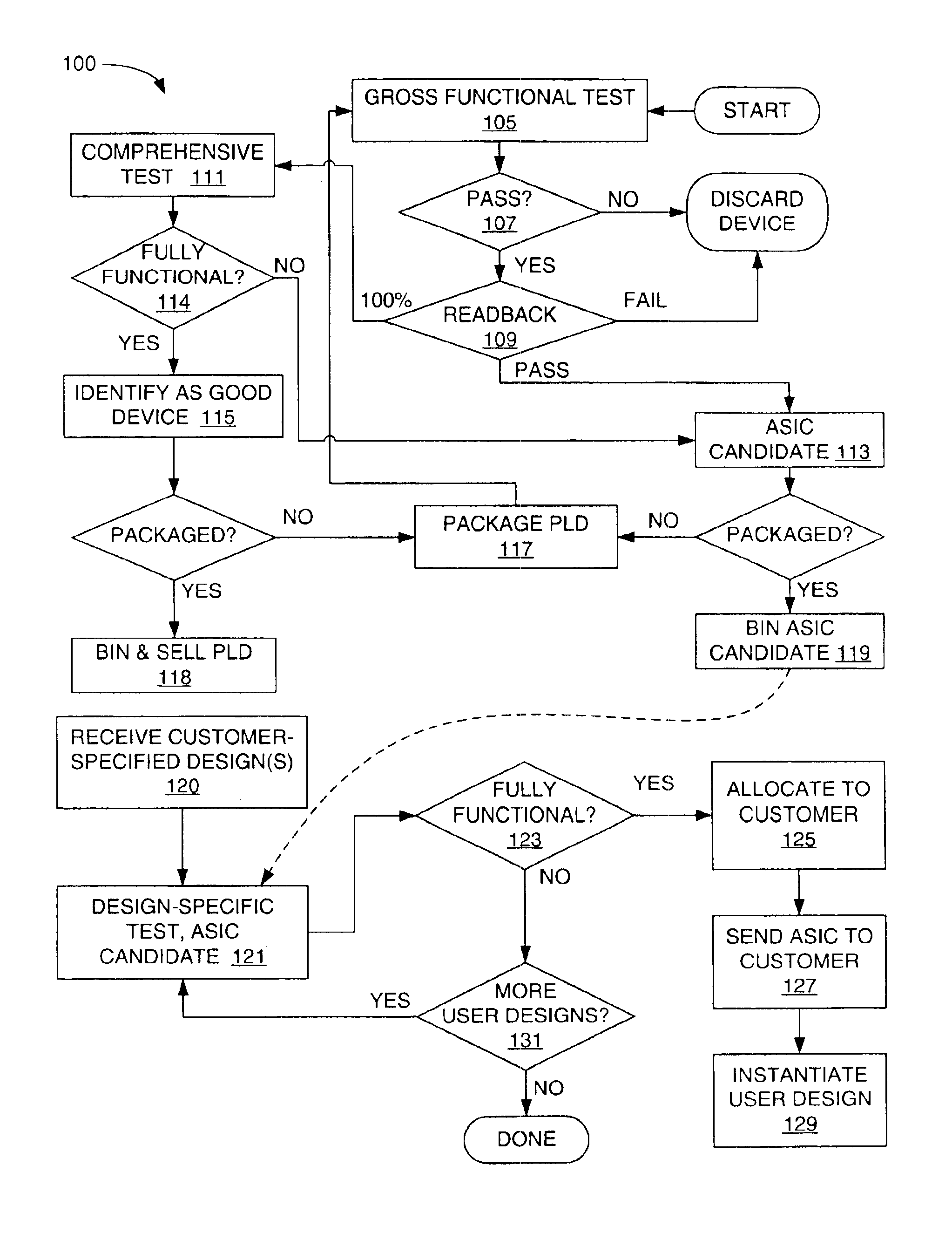
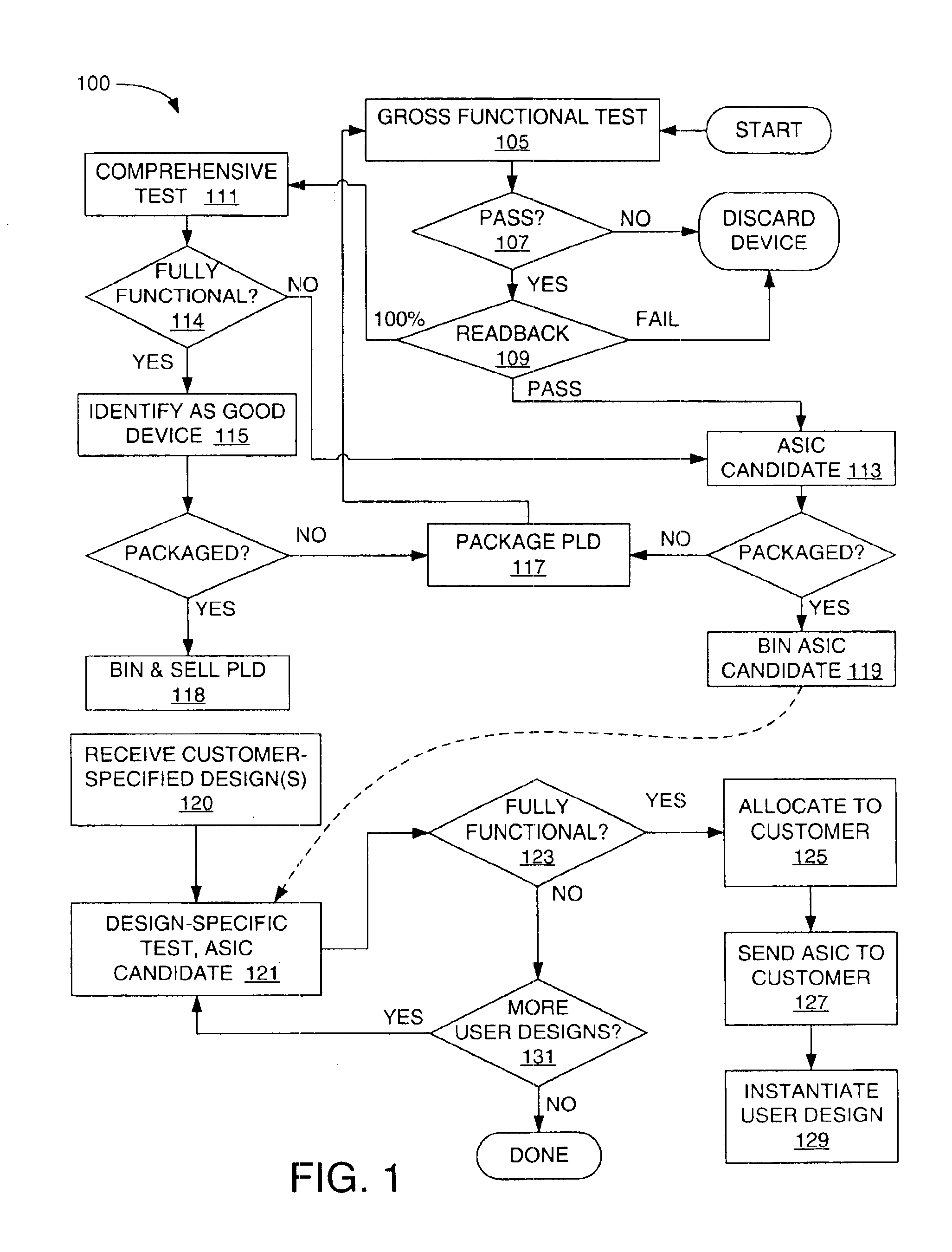
[0038]FIG. 1 is a flow chart 100 showing one embodiment of the present invention as applied to FPGAs. Subsequent to fabrication, the various chips on a given semiconductor wafer are tested for “gross” defects (step 105). For purposes of the present disclosure, “gross” defects are defects that have a high probability of rendering a PLD unfit for any customer purpose. Examples of gross defects include power-supply shorts, opens, excessive leakage, defective clock-management circuitry, and significant numbers of defectiv...


PUM


Abstract

Disclosed are methods for utilizing programmable logic devices that contain at least one localized defect. Such devices are tested to determine their suitability for implementing selected designs that may not require the resources impacted by the defect. If the FPGA is found to be unsuitable for one design, additional designs may be tested. The test methods in some embodiments employ test circuits derived from a user's design to verify PLD resources required for the design. The test circuits allow PLD vendors to verify the suitability of a PLD for a given user's design without requiring the PLD vendor to understand the user's design.

Description

[0001]This is a continuation application of U.S. Ser. No. 10 / 104,324 filed Mar. 22, 2002, now U.S. Pat. No. 6,817,006, which is a continuation-in-part of U.S. Ser. No. 09 / 924,365 filed Aug. 7, 2001.CROSS-REFERENCE TO RELATED APPLICATIONS[0002]This application claims priority under 35 U.S.C. §119(e) from U.S. Pat. No. 6,664,808 B2 entitled “A METHOD OF USING PARTIALLY DEFECTIVE PROGRAMMABLE LOGIC DEVICES,” by Zhi-Min Ling et al., issued on Dec. 16, 2003, which is incorporated herein by reference.FIELD OF THE INVENTION[0003]The present invention relates to programmable logic devices, and more particularly to methods for testing and using programmable logic devices that contain minor defects.BACKGROUND OF THE INVENTION[0004]Programmable logic devices (PLDs), such as field-programmable gate arrays (FPGAs), are user-programmable integrated circuits that can be programmed to implement user-defined logic circuits. In a typical architecture, an FPGA includes an array of configurable logic b...

Claims


Application Information

Patent Timeline
Patent Type & Authority Patents(United States)
IPC IPC(8): G01R31/28G01R31/3185G06F17/50H01L21/82
CPCG06F17/5054G01R31/318519G06F30/34
Inventor WELLS, ROBERT W.LING, ZHI-MINPATRIE, ROBERT D.TONG, VINCENT L.CHO, JAETOUTOUNCHI, SHAHIN
Owner XILINX INC
Why Eureka
Try Eureka