Apparatus and method for inspecting picture elements of an active matrix type display board

a technology of active matrix type and display board, which is applied in the direction of identification means, instruments, computing, etc., can solve the problems of large expense, inability to reliably inspect the picture elements of the active matrix type display board, and inability to ensure the accuracy of the inspection results, etc., and achieve the effect of enhancing the accuracy of inspection results

Inactive Publication Date: 2005-05-10
WINTEST CORP
View PDF11 Cites 15 Cited by
  • Summary
  • Abstract
  • Description
  • Claims
  • Application Information

AI Technical Summary

Benefits of technology

[0027]With the foregoing problems in view, it is an object of the present invention to provide an apparatus and a method for inspecting picture elements of an active matrix type display, which, when inspecting an active matrix type display based on either an LCD array device or an EL array device, is capable of enhancing the accuracy thereof.

Problems solved by technology

In this inspection, a problem is that if the product is not assembled into its final form, an image cannot be displayed, and consequently, large expenses are incurred for nothing when a defect occurs, and, in addition, another problem is that inspection results are not reliable due to the fact that, because they are subjective inspections done by the naked eye, the evaluation criteria used by various inspectors are apt to lack uniformity, and inspection accuracy can be off the mark as a result of human fatigue.
However, the problem is that, in LCD display devices or EL display devices currently being developed, due to the high-temperature polysilicon processes and the low-temperature polysilicon processes which have come to be used in recent years, the irregularities in the characteristics of various elements inside a device resulting from manufacturing process-related problems are great.
However, the problem is that, in polysilicon liquid crystal display 1 according to LCD display devices manufactured by either a high-temperature polysilicon process or a low-temperature polysilicon process, there are large characteristic irregularities in the various elements internal thereto due to problems related to the manufacturing process.
In particular, irregularities in the elements of source switches 13 (A1-A9) cannot be ignored, and the vertical stripes of when sampling a waveform outputted to an inspection device, which are the cause of these relatively large irregularities in source switches 13, are a big problem, and in an inspection method, wherein the absolute quantity of a read-out charge is evaluated simply, since there are numerous cases in which the side of the noise level resulting from these irregularities is larger than the level of the inspection signal, the results pose problems from the standpoint of inspection accuracy.
Moreover, the problem is that, in line with making LCD and EL devices larger in recent years, each of these nonuniform items is moving in a direction in which the degree of this nonuniformity is increasing.
A problem is that this crosstalk problem is becoming more apt to occur in line with making the polysilicon liquid crystal display 1 larger and higher in density.
Furthermore, when the noise originating in device drive signals from horizontal driving circuit 4 and vertical driving circuit 5, as well as the level of irregularities in each element of a test head or measurement device (not shown in the figure) is larger than a picture element inspection signal, there is the problem that the picture element inspection signal gets buried between such noise or irregularities levels, making detection impossible.

Method used


Image

  • Apparatus and method for inspecting picture elements of an active matrix type display board
  • Apparatus and method for inspecting picture elements of an active matrix type display board
  • Apparatus and method for inspecting picture elements of an active matrix type display board

Examples


Embodiment Construction

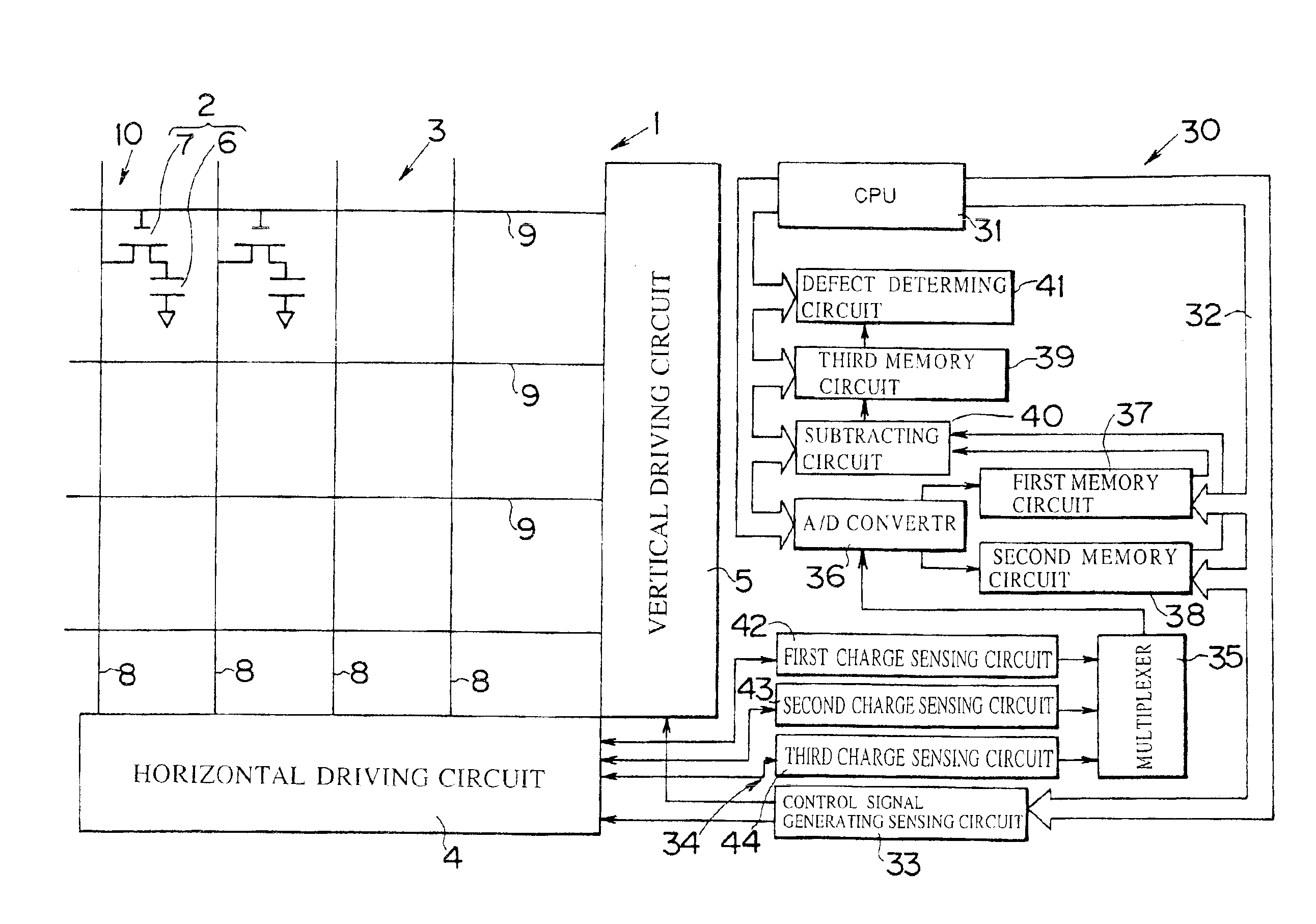
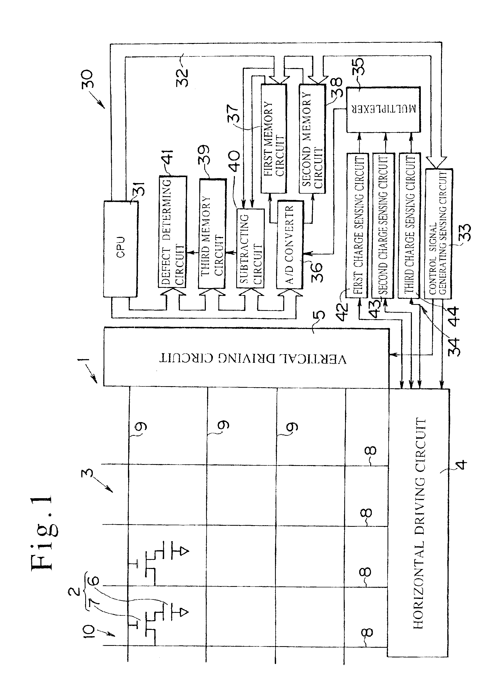
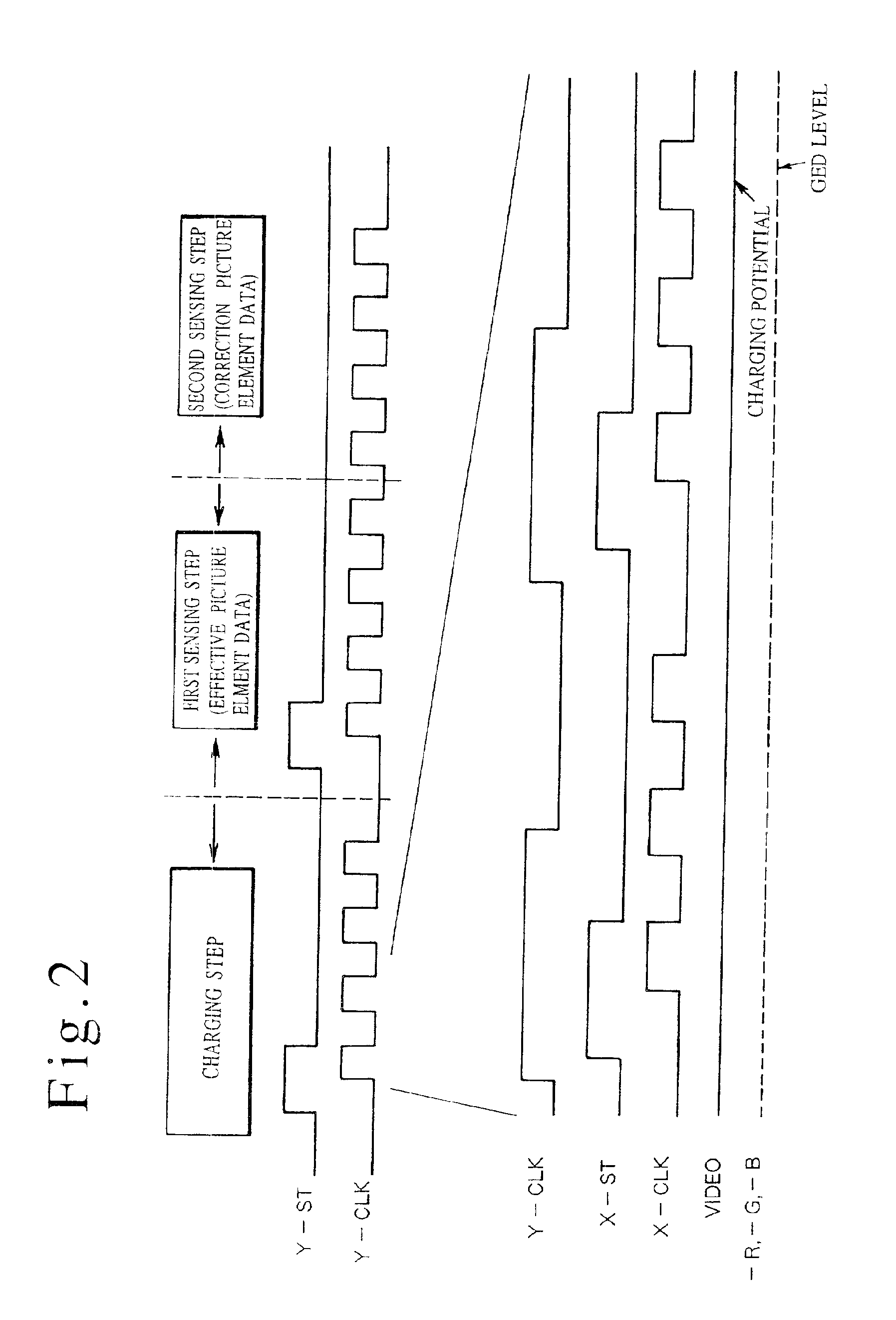
[0059]Next, a picture element inspecting apparatus 30 for an active matrix type display according to aspects of the embodiment of the present invention will be explained together with methods for inspecting these picture elements based on FIG. 1 through FIG. 5. However, the same reference numerals will be assigned to parts that are the same as those in FIG. 6, and detailed explanations thereof will be omitted.

[0060]FIG. 1 is a block diagram of a picture element inspection apparatus 30, and picture element inspection apparatus 30 has a central processing unit 31 (CPU), a control bus 32, a control signal generating circuit 33, a charge sensing circuit 34, a multiplexer 35, an A / D converter 36, a first memory circuit 37, a second memory circuit 38, and a third memory circuit 39, a subtracting circuit 40 (arithmetic circuit), and a defect determining circuit 41.

[0061]Central processing unit 31 (CPU) controls the entire apparatus via control bus 32.

[0062]Control signal generating circuit...


PUM

PropertyMeasurementUnit
temperatureaaaaaaaaaa
resistanceaaaaaaaaaa
capacitanceaaaaaaaaaa

Abstract

The present invention provides a picture element inspecting apparatus and method for an active matrix type display that is constituted by an LCD array device or an EL array device, which is capable of canceling the irregularities in source switches 13, the noise caused by device driving signals, and the irregularities in devices in the measurement apparatus, and enhancing the accuracy of a picture element inspection. The present invention is based on the finding that irregularities in the direction of the source lines 8 can be canceled by performing, in addition to a charging step and first sensing step that are realized by the charging and discharging of picture elements 2, a second sensing step in a state where gate lines are not selected, and subtracting correction picture element data thus obtained, and is characterized in that a subtraction operation is performed on effective picture element data obtained by electrically charging picture elements 2, and correction picture element data obtained in a state where gate lines 9 of picture elements 2 are not selected, and the quality of the picture elements 2 is determined based on the subtraction output.

Description

BACKGROUND OF THE INVENTION[0001]1. Field of the Invention[0002]The present invention is related to an apparatus and method for inspecting the picture elements of an active matrix type display, and more particularly to an apparatus and method for inspecting the picture elements of an active matrix type display, which is capable of enhancing picture element inspection accuracy upon picture element inspection of a liquid crystal display array (LCD array) or organic electro luminescent display array (EL array) having active matrix structures by canceling source switching element irregularities, measurement noise attributed to device drive signals, and irregularities in various elements in the measurement system.[0003]2. Description of the Related Art[0004]A conventional LCD array device and EL array device were assembled into respective modules, and a 100% inspection was performed by human visual observation.[0005]In this inspection, a problem is that if the product is not assembled in...

Claims


Application Information

Patent Timeline
Patent Type & Authority Patents(United States)
IPC IPC(8): G09G3/36G02F1/1368G02F1/13G09F9/00G09F9/30G09G3/00
CPCG09G3/006G09G2300/08G09G3/3648G02F1/13
Inventor NARA, SHOUJIITOH, MASATOSHIOOKUMA, MAKOTO
Owner WINTEST CORP
Why Eureka
Try Eureka