
Method of forming a dual damascene interconnect by selective metal deposition

a damascene interconnect and metal deposition technology, applied in the direction of semiconductor devices, semiconductor/solid-state device details, electrical apparatus, etc., can solve the problems of aluminum not being able to adequately fill the contact openings by conventional physical vapor deposition (pvd) sputtering, copper showing even lower resistivity,

Inactive Publication Date: 2005-05-17
ROUND ROCK RES LLC
View PDF19 Cites 13 Cited by
  • Summary
  • Abstract
  • Description
  • Claims
  • Application Information

AI Technical Summary

Benefits of technology

[0009]These and other needs are satisfied b

Problems solved by technology

Copper demonstrates even lower resistivity, though it introduces its own difficulties in integration.
Contact openings, however, are being developed with higher aspect ratios (A / R), such that aluminum can not adequately fill the contact openings by conventional physical vapor deposition (PVD) sputtering.
Imperfect aluminum deposition also results in electromigration at points of inadequate fill, especially in the contact regions where there are generally large current densities.
Furthermore, Al—Si contact interfaces are prone to junction spiking resulting in large leakage currents or even electrical shorts.
Moreover, separate plug and wiring formation is less efficient than simultaneous formation using dual damascene process flows.

Method used


Image

  • Method of forming a dual damascene interconnect by selective metal deposition
  • Method of forming a dual damascene interconnect by selective metal deposition
  • Method of forming a dual damascene interconnect by selective metal deposition

Examples


Embodiment Construction

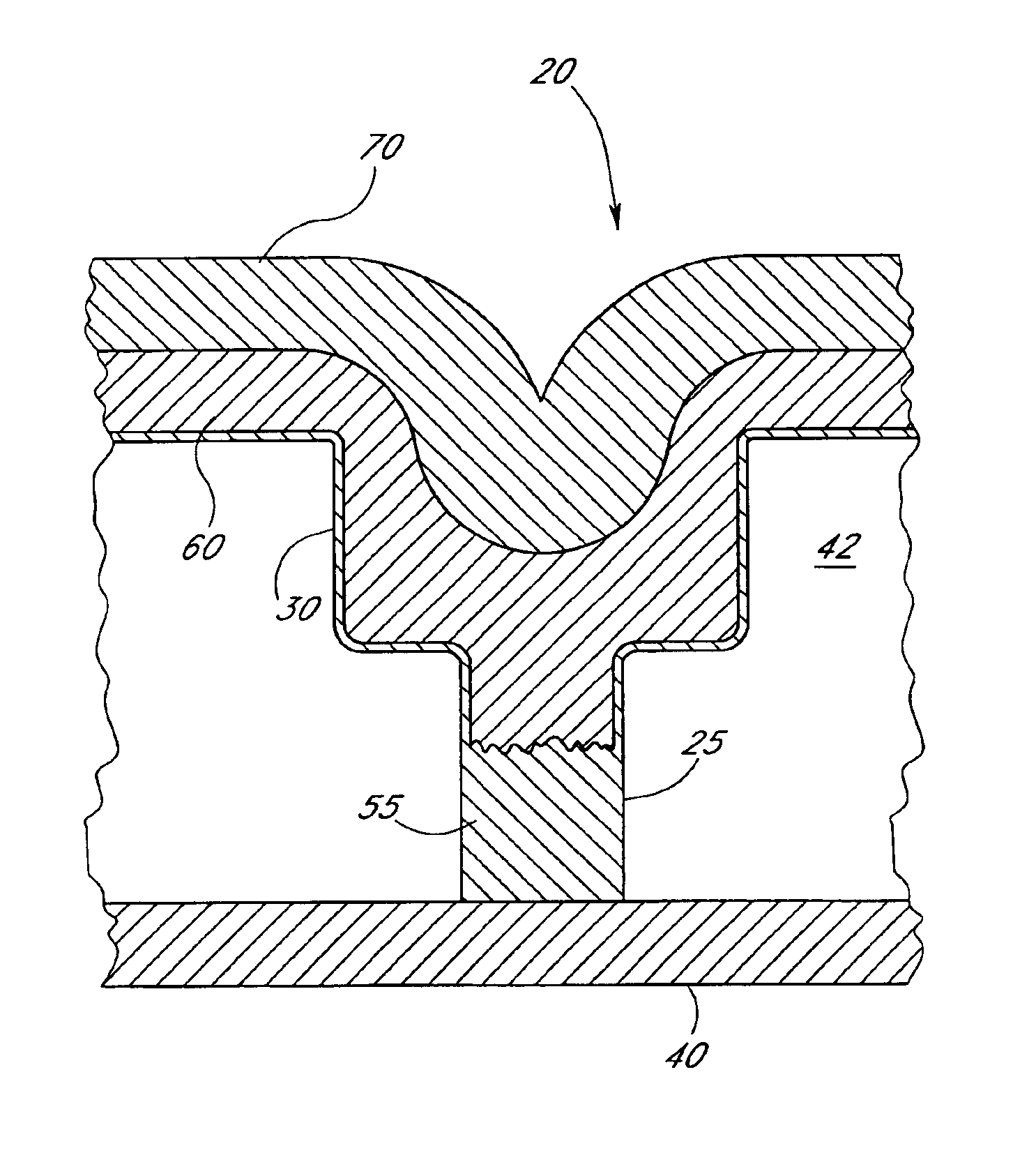
[0024]The preferred embodiments are illustrated in the context of metallization processes in an integrated circuit, including contact plug formation and damascene processes, where selective tungsten (W) partially fills a void and aluminum is sputtered thereover. The skilled artisan will readily appreciate, however, that the materials and methods disclosed herein will have application in a number of other contexts where contact openings are partially filled with a first conductive layer, desirably followed by a more suitable subsequent conductive layer.

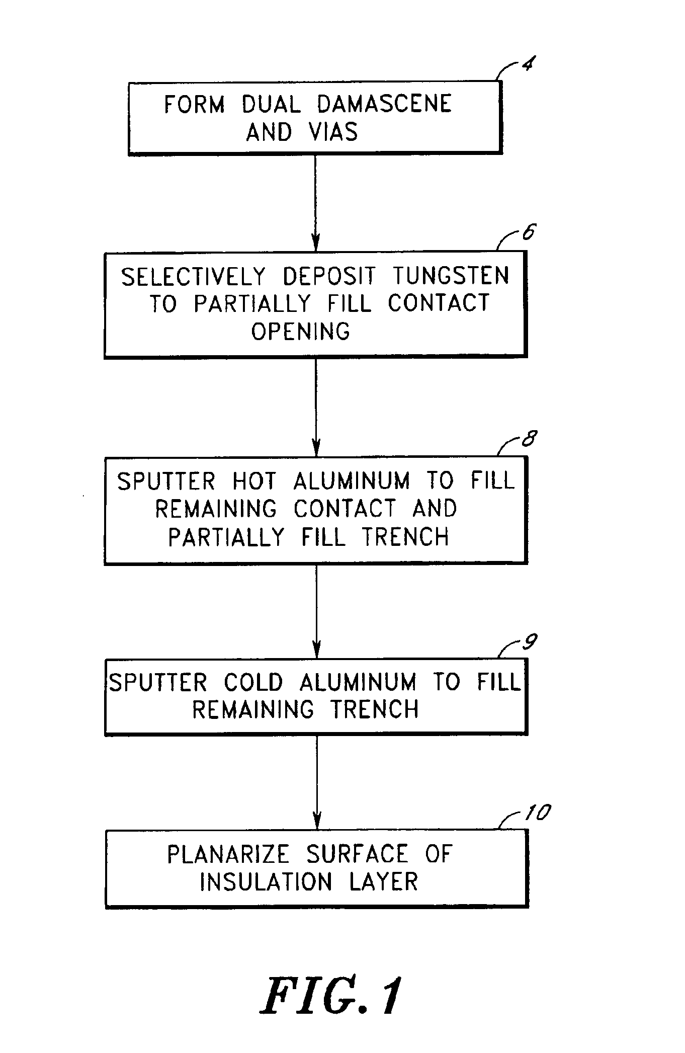
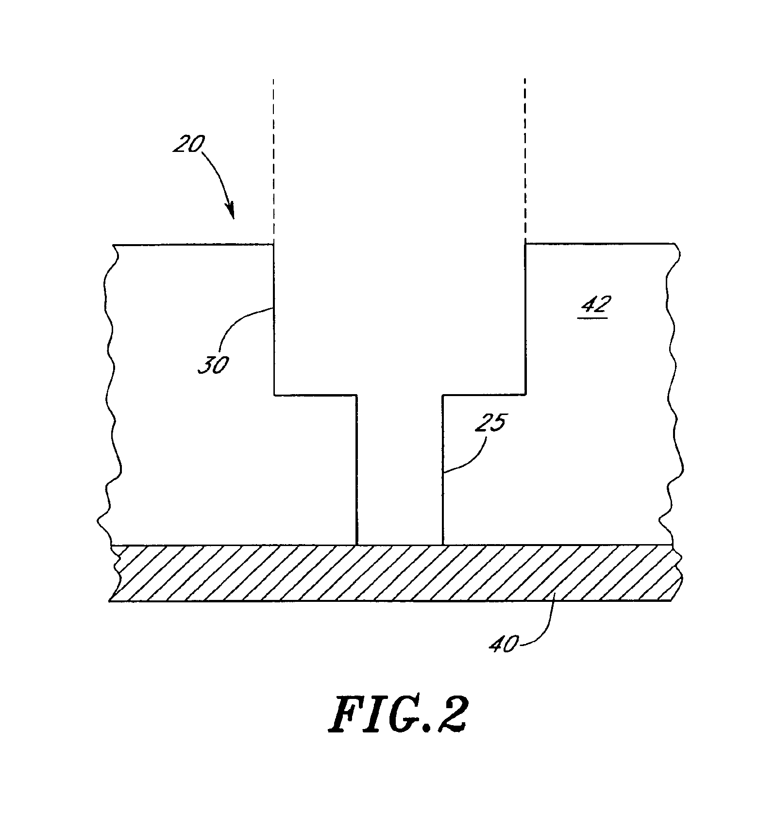
[0025]FIG. 1 schematically illustrates a process flow for forming a partial contact plug over which further metal can be deposited in accordance with a preferred embodiment of the invention. As shown, the process begins with formation 4 of a dual damascene structure comprising trenches and vias. The trenches and vias may be formed using conventional photolithography and etch technologies.

[0026]While not shown, the skilled artisan will ...


PUM


Abstract

A dual damascene process is disclosed, in which a contact via and trench pattern is etched into insulating layer(s). The via is first partially filled by selective metal (e.g., tungsten) deposition, thereby forming a partial plug that raises the floor and reduces the effective aspect ratio of the trench and via structure. The remaining portion of the contact via is then filled with a more conductive material (e.g., aluminum). This deposition also at least partially fills the overlying trench to form metal runners. In the illustrated embodiment, hot aluminum deposition fills the portion of the contact via left unoccupied by the selective deposition and overfills into the trench. A further, cold aluminum deposition then follows, topping off the trench prior to planarization. The dual damascene structure thus exhibits a raised floor relative to conventional dual damascene metallization, while still retaining the conduction benefits of aluminum through a significant portion of the contact and the metal runner formed in the trench.

Description

REFERENCE TO RELATED APPLICATION[0001]This application is a divisional of application Ser. No. 09 / 548,472, filed Apr. 13, 2000 U.S. Pat. No. 6,534,866.FIELD OF THE INVENTION[0002]The present invention relates generally to the fabrication of multi-layer integrated circuits, and more particularly to contact formation in a dual damascene interconnect scheme.BACKGROUND OF THE INVENTION[0003]There are numerous semiconductor process steps involved in the development of modem day integrated circuits (ICs). From the initial fabrication of silicon substrates to final packaging and testing, integrated circuit manufacturing involves many fabrication steps, including photolithography, doping, etching and thin film deposition. As a result of these processes, integrated circuits are formed of microscopic devices and wiring amid multiple layers.[0004]Contact vias or openings are commonly formed in insulating materials known as interlevel dielectrics (ILDs). The vias are then filled with conductive...

Claims


Application Information

Patent Timeline
IPC IPC(8): H01L21/02H01L21/4763H01L21/44H01L23/48H01L21/285H01L21/768
CPCH01L21/76879H01L21/76877H01L21/28562
Inventor TRIVEDI, JIGISH D.VIOLETTE, MIKE P.
Owner ROUND ROCK RES LLC
Learn More