Soft error resistant semiconductor device

a semiconductor device and error-resistant technology, applied in semiconductor devices, semiconductor/solid-state device details, electrical devices, etc., can solve problems such as reducing reliability, limiting the applicability of devices, and error in reading storage contents, so as to reduce radiation-induced charge-carrier generation

Inactive Publication Date: 2005-05-17
GLOBALFOUNDRIES US INC
View PDF7 Cites 19 Cited by
  • Summary
  • Abstract
  • Description
  • Claims
  • Application Information

AI Technical Summary

Benefits of technology

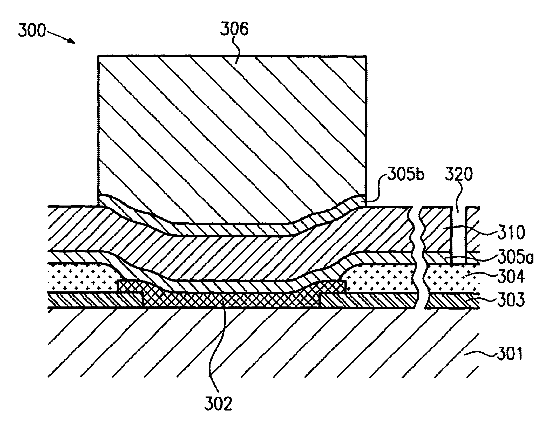
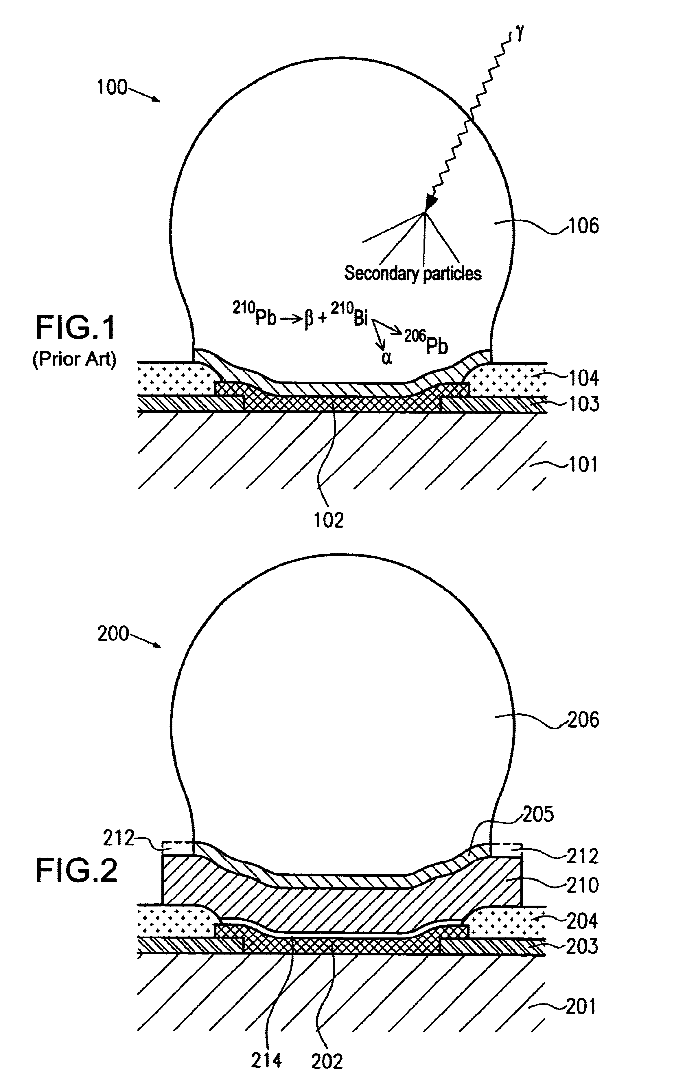
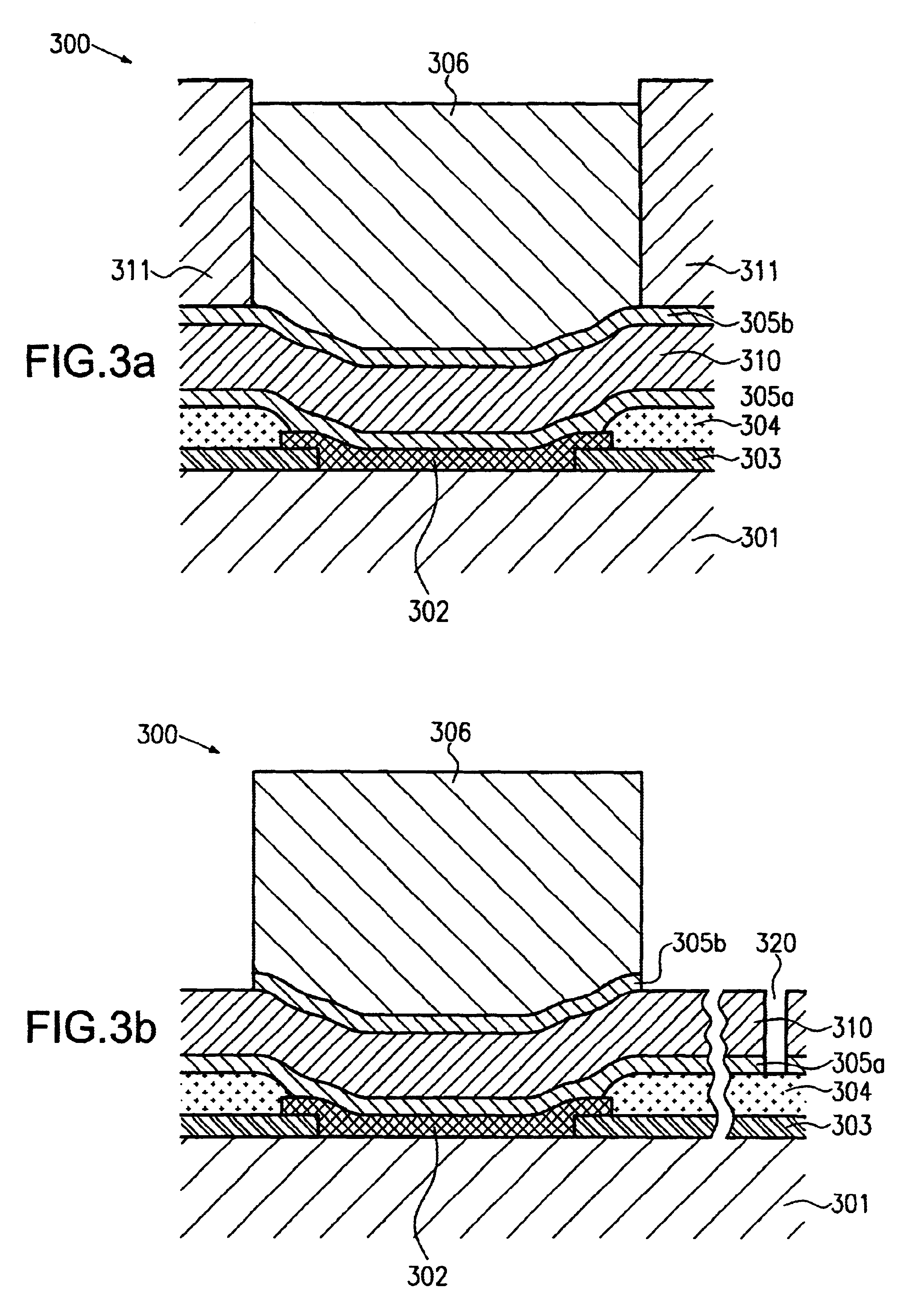
[0014]To reduce radiation induced charge-carrier generation, the present invention provides, according to one embodiment, a semiconductor device comprising a substrate including a contact pad and a solder bump formed on the contact pad. Moreover, an absorption layer is disposed between the contact pad and the solder bump, wherein a thickness of the absorption layer is configured to substantially completely stop alpha particles of at least 5.4 MeV.
[0015]According to a further embodiment of the present invention, a semiconductor device comprises a substrate including a contact pad and a solder bump formed on the contact pad. An underbump metallization is disposed between the contact pad and the solder bump, wherein the underbump metallization substantially prevents diffusion of solder bump material into the substrate and provides adhesion of the solder bump to the substrate. The underbump metallization has a thickness that is sufficient to stop alpha particles having an energy of approximately 5.4 MeV.

Problems solved by technology

Due to the ever decreasing feature sizes of modern integrated circuits, however, radiation-induced charge carrier generation in semiconductor devices increasingly proves to be a possible source of failure for the device, which accordingly decreases reliability, or even causes a complete failure, and thus restricts applicability of the device.
High energetic particles penetrating the semiconductor device may create a plurality of electron hole pairs, which may then enter charge-sensitive areas and cause device failures, and / or may accumulate in charge-sensitive regions of the semiconductor device, for example in dielectrics of storage capacitors or in gate insulation layers of MOS transistors.
In the latter case, a significant drift in the threshold voltage of the transistor device may be created, whereas an accumulated charge in a storage capacitor may lead to a changed logic state of the capacitor, thereby causing an error in reading the storage contents, which is also referred to as soft error.
Although this approach allows effective absorption of alpha particles emitted by the low cost lead, the provision of low alpha lead is costly and it is difficult during the reflowing of the solder bump for forming a solder ball to avoid mixing of the low alpha lead and the low cost lead.
In this arrangement, the penetration of alpha particles is significantly reduced, wherein, however, the penetration of alpha particles, inherently created by the decay of alpha active isotopes that are moving directly from the solder bump into the underlying device regions, may not be stopped efficiently.
Consequently, this additional charge may cause a significant shift of the operating conditions, especially when the feature sizes are small and the corresponding operating voltages are low.

Method used


Image

  • Soft error resistant semiconductor device
  • Soft error resistant semiconductor device
  • Soft error resistant semiconductor device

Examples


Embodiment Construction

[0023]Illustrative embodiments of the invention are described below. In the interest of clarity, not all features of an actual implementation are described in this specification. It will of course be appreciated that in the development of any such actual embodiment, numerous implementation-specific decisions must be made to achieve the developers' specific goals, such as compliance with system-related and business-related constraints, which will vary from one implementation to another. Moreover, it will be appreciated that such a development effort might be complex and time-consuming, but would nevertheless be a routine undertaking for those of ordinary skill in the art having the benefit of this disclosure.

[0024]The present invention will now be described with reference to the attached figures. Although the various regions and structures of a semiconductor device are depicted in the drawings as having very precise, sharp configurations and profiles, those skilled in the art recogni...


PUM

PropertyMeasurementUnit
thicknessaaaaaaaaaa
thicknessaaaaaaaaaa
thicknessaaaaaaaaaa

Abstract

A semiconductor device comprises a material layer adapted to efficiently stop alpha particles that are substantially generated within a solder bump of a flip chip device. The materials used for stopping the alpha particles are compatible with standard back-end processing and do not degrade adhesion of the solder bump to the remaining substrate. Moreover, a low electrical resistance is maintained and heat dissipation may be improved.

Description

BACKGROUND OF THE INVENTION[0001]1. Field of the Invention[0002]The present invention relates to a semiconductor device that exhibits an increased resistance against radiation-induced malfunctions, and, more particularly, to a semiconductor device having a reduced penetration rate of alpha particles.[0003]2. Description of the Related Art[0004]Steadily decreasing feature sizes in modern integrated circuits allow fabrication of electronic devices exhibiting complex functionality within an extremely small volume. Accordingly, modern integrated circuits are increasingly used in all types of electronic devices as data processing units or as storage media, irrespective of whether the device is an everyday product, such as a personal computer, or a device employed in the medical, technical or scientific fields. Among this variety of possible applications of integrated circuits, certain critical applications, e.g., data processing units in vehicles, medical devices and the like, require ex...

Claims


Application Information

Patent Timeline
Patent Type & Authority Patents(United States)
IPC IPC(8): H01L23/552H01L23/485H01L23/556H01L23/48
CPCH01L23/556H01L24/03H01L24/05H01L2924/0002H01L2924/13091H01L2224/05572H01L2224/13007H01L2924/00014H01L24/12H01L2224/03912H01L2224/0401H01L2224/05568H01L2224/05599H01L2224/10126H01L2224/1147H01L2224/16H01L2924/01013H01L2924/01014H01L2924/01022H01L2924/01028H01L2924/01029H01L2924/01047H01L2924/01073H01L2924/01074H01L2924/01078H01L2924/01079H01L2924/01082H01L2924/014H01L2924/04941H01L2924/04953H01L2924/05042H01L2924/14H01L2924/19041H01L2924/19043H01L2924/3025H01L2924/01024H01L2924/01033H01L2924/01068H01L2924/01084H01L2224/05552H01L2924/00
Inventor SCHAMMLER, GISELABOTTCHER, MATHIASKUECHENMEISTER, FRANKGEHRE, DANIELZSCHECH, EHRENFRIED
Owner GLOBALFOUNDRIES US INC
Why Eureka
Try Eureka