Waveguide and method of smoothing optical surfaces

a waveguide and optical surface technology, applied in waveguides, bundled fibre light guides, instruments, etc., can solve the problems of inability to actually blacken direct view images, cumbersome screens, and a practical limit for cathode ray tubes, and achieve excellent viewability without excessive grinding and polishing of surfaces

Inactive Publication Date: 2005-05-17
SKC HAAS DISPLAY FILMS CO LTD
View PDF10 Cites 364 Cited by
  • Summary
  • Abstract
  • Description
  • Claims
  • Application Information

AI Technical Summary

Benefits of technology

[0009]The invention provides improved waveguides that provide excel...

Problems solved by technology

Conventional cathode ray tubes have a practical limit in size, and are relatively deep to accommodate the required electron gun.
However, such screens have various viewing shortcomings including limited viewing angle, resolution, brightness, and contrast, and such screens are typically relatively cumbersome in weight and shape.
However, it is impossible for direct view CRTs to actually be black because they utilize phosphors to form images, and those phosphors are non-black.
However, optical waveguides of the step index cladding type that are stacked and fused together have some significant drawbacks.
Handling and cutting many strips of thin polymer is very difficult.
The compatibility of materials that have a refractive index difference from core to clad is limited.
This may contribute to problems such as inadequate adhesion between layers.
Such incompatibility may result in layer to layer interface problems such as air gaps, rough surfaces, or layer separation.
These types of problems may cause a loss of light at each bounce at the interface between the core layer and surrounding cladding layers.
Furthermore when stacked, fused and saw cut, pan...

Method used


Image

  • Waveguide and method of smoothing optical surfaces
  • Waveguide and method of smoothing optical surfaces
  • Waveguide and method of smoothing optical surfaces

Examples


examples

[0083]The materials used in the examples and comparative samples of the invention include the following.

Example of Waveguide Component

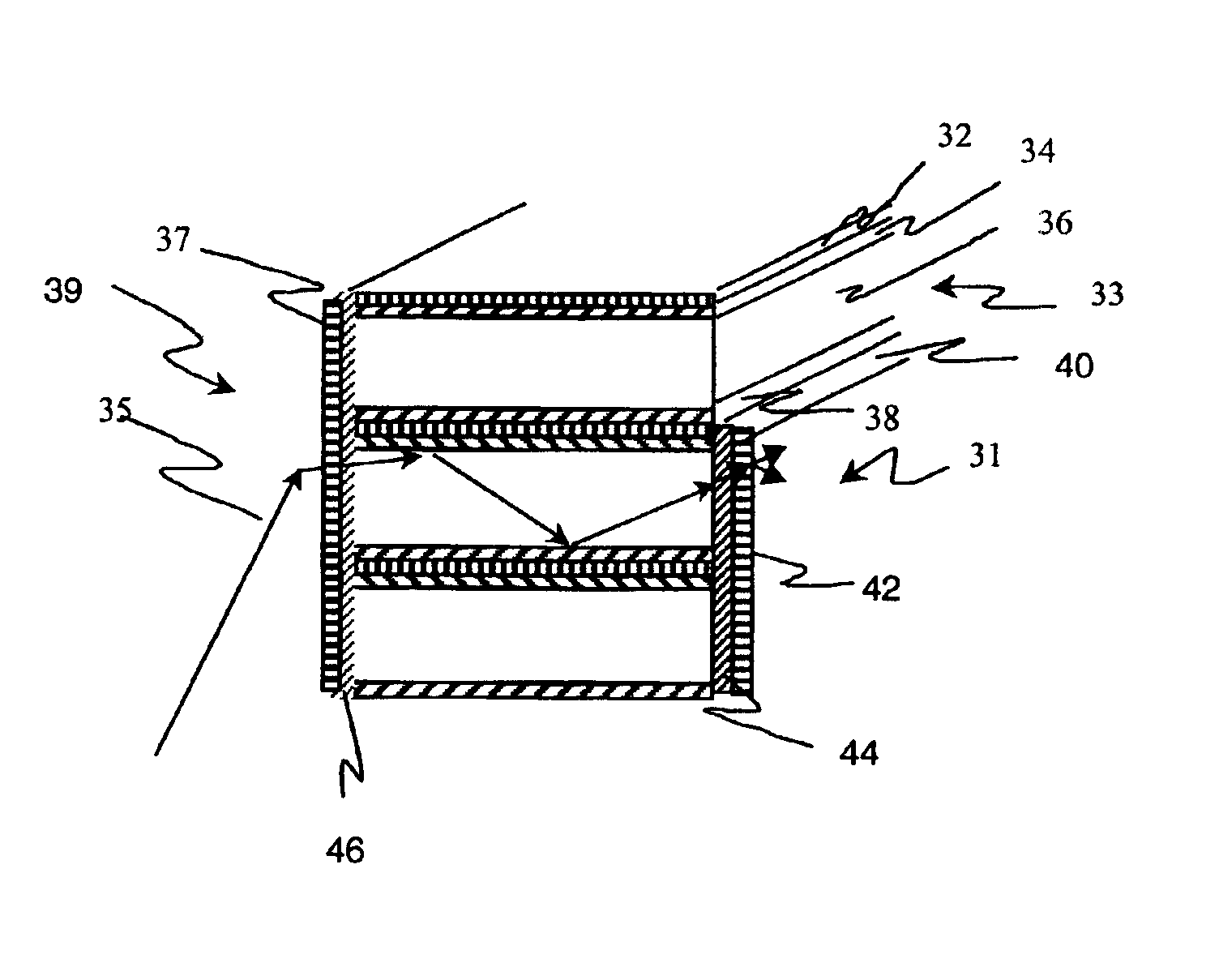
[0084]A waveguide component as per the present invention is constructed as follows.

[0085]The core of the waveguide component comprises a ˜254 μM thick polycarbonate clear base. On each side of the polycarbonate base is coated a ˜3 μm thick (dry) clad layer comprising an epoxy resin (EPON 1009F) manufactured by Shell. The coating is made from a solution in 2-butanone, using a fixed-slot extrusion hopper, and thoroughly dried. A second coating layer was applied on top of each side the EPON clad which serves as an adhesive layer. This layer is approximately 4.5 μm thick. The layer consists of VITEL 2700 polyester (supplied by Bostik) with a black dye (Solvent Black 27) mixed in at approximately 12.5% of the solids. The optical density of the layer is approximately 0.8 as measured by X-rite densitometer. The coating is made from a solution in 2-butanone, ...


PUM


Abstract

Disclosed is a waveguide having a light inlet surface and a viewing surface comprising stacked core layers separated by clad layers to form channels and bearing a smoothing layer on at least one of the light inlet surface or the viewing surface thereof.

Description

FIELD OF THE INVENTION[0001]This invention relates to a stacked waveguide having a light inlet surface and a viewing surface bearing a smoothing layer on at least one of the light inlet surface or the viewing surface thereof, and a method of making a display screen.BACKGROUND OF THE INVENTION[0002]Optical screens typically use cathode ray tubes (CRTs) for projecting images onto the screen. The standard screen has a width to height ratio of 4:3 with 525 vertical lines of resolution. An electron beam is scanned both horizontally and vertically across the screen to form a number of pixels, which collectively form the image.[0003]Conventional cathode ray tubes have a practical limit in size, and are relatively deep to accommodate the required electron gun. Larger screens are available which typically include various forms of image projection. However, such screens have various viewing shortcomings including limited viewing angle, resolution, brightness, and contrast, and such screens ar...

Claims


Application Information

Patent Timeline
IPC IPC(8): G02B6/06G02B6/08
CPCG02B6/08Y10S385/901
Inventor AYLWARD, PETER T.SMITH, THOMAS M.SLATER, DANIEL A.RAM, ARUNACHALAM T.
Owner SKC HAAS DISPLAY FILMS CO LTD
Why Eureka
Try Eureka