Wafer holding ring for chemical and mechanical polisher
- Summary
- Abstract
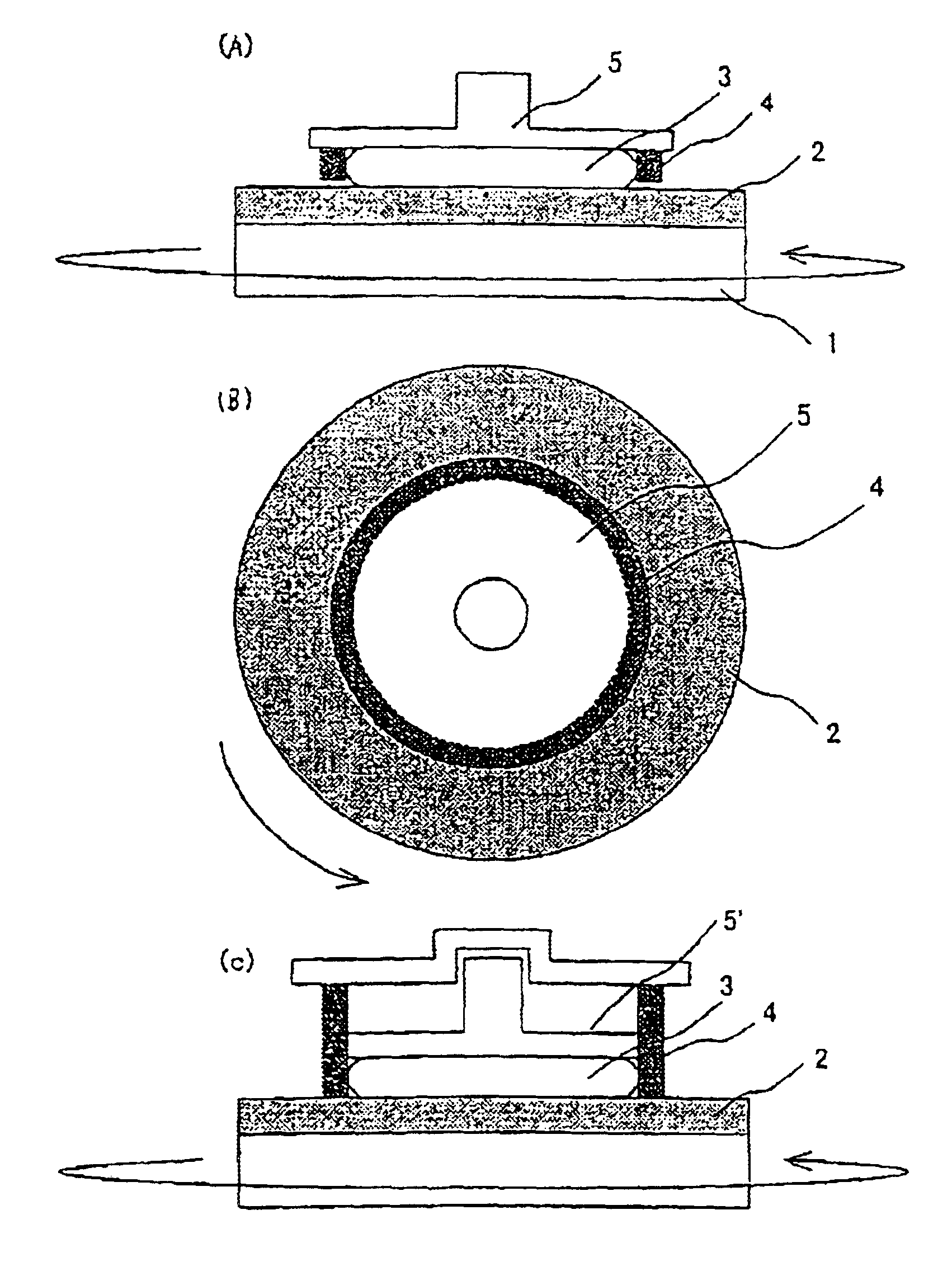
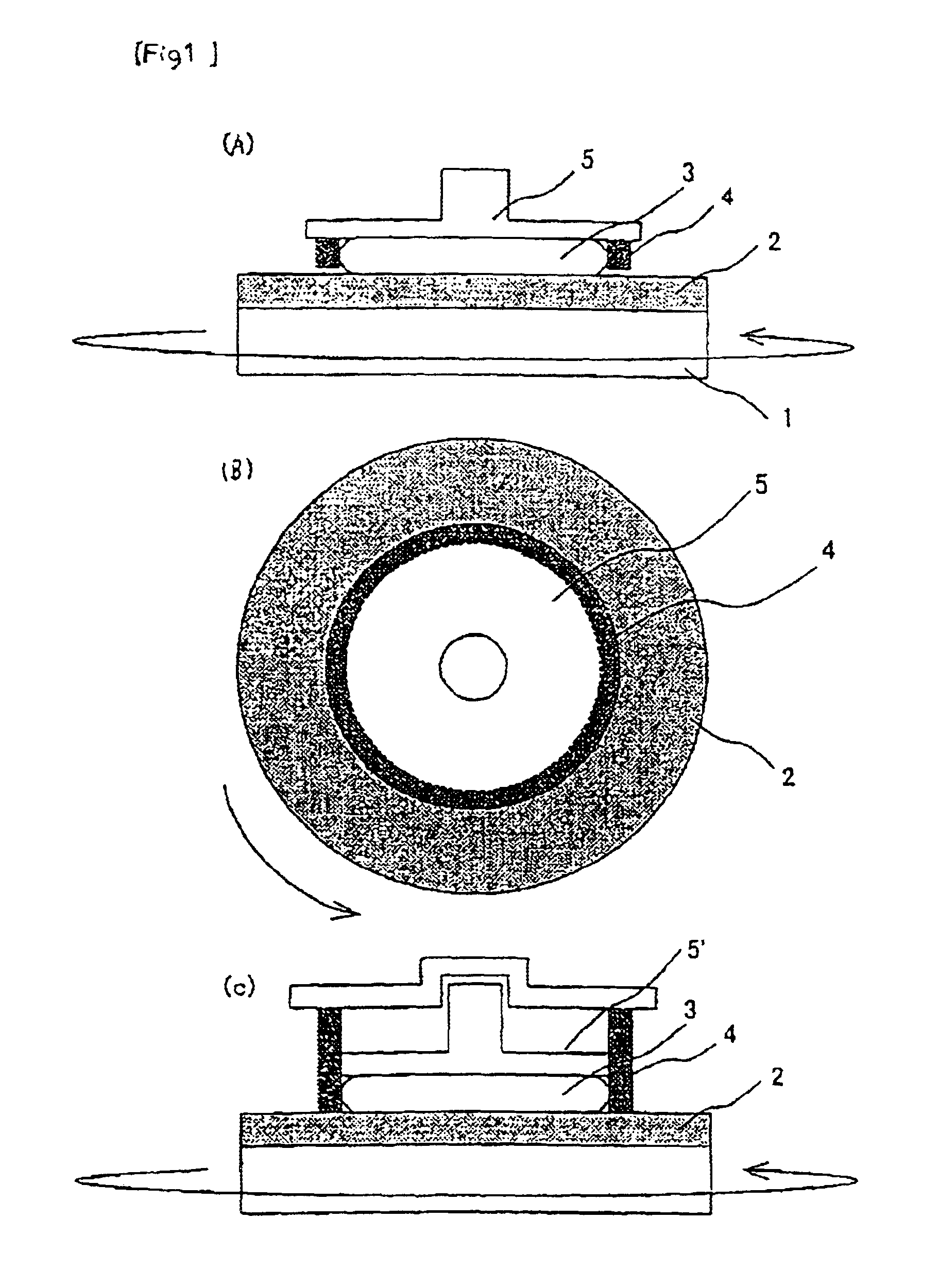
- Description
- Claims
- Application Information
AI Technical Summary
Benefits of technology
Problems solved by technology
Method used
Image

Examples
example
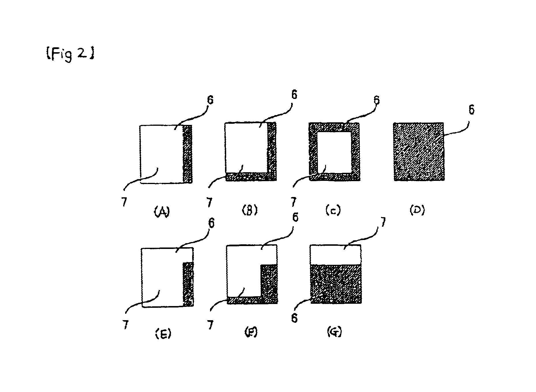
[0073]Materials for wafer-holding ring for CMP apparatuses were evaluated for abrasion resistance.
[0074]Columnar materials having a size of 11.3 mmØ×10 mm formed of the following materials a to h were provided as specimens. A projected portion having a thickness of 500 to 800 μm was provided on one plane of each of the columnar materials. The projected portion was brought into contact with a counter material immersed in a slurry and was rotated while applying a load to the specimen to measure the abrasion loss. The abrasion loss was evaluated in terms of the degree of a reduction in height of the projected portion (μm) and the degree of a reduction in central sectional area (μm2) of the projected portion. Further, the sectional form after the abrasion was inspected.[0075]Testing conditions were as follows.[0076]Contact pressure: 300 g / cm2 [0077]Peripheral velocity: 0.9 m / sec[0078]Abrasion time: 8 hr[0079]Slurry used: Acidic slurry, W 2000, manufactured by CABOT Corporation Alkaline ...
PUM
 Abstract
Description
Claims
Application Information
 - R&D Engineer
- R&D Manager
- IP Professional
- Industry Leading Data Capabilities
- Powerful AI technology
- Patent DNA Extraction
Browse by: Latest US Patents, China's latest patents, Technical Efficacy Thesaurus, Application Domain, Technology Topic.
© 2024 PatSnap. All rights reserved.Legal|Privacy policy|Modern Slavery Act Transparency Statement|Sitemap