Fabrication of nanometer size gaps on an electrode

a nano-gap, electrode technology, applied in the direction of instruments, photo-taking processes, photomechanical devices, etc., can solve the problems of low yield, complex early methods for producing nano-gaps, and the building blocks of future electronic devices will be found in such systems

Inactive Publication Date: 2005-05-24
THE TRUSTEES OF THE UNIV OF PENNSYLVANIA
View PDF2 Cites 44 Cited by
  • Summary
  • Abstract
  • Description
  • Claims
  • Application Information

AI Technical Summary

Benefits of technology

[0008]The present method fabricates metallic wires or electrodes with nanometer size breaks (nanogaps), which are ideal for use as metallic connections to molecular electronic circuits or circuits containing other nanometer size clusters. The method is scaleable, allowing the formation of many nanogaps. By using functional NTs in this self-assembly process, multiple electrodes with nanogaps can be fabricated simultaneously in controlled locations.

Problems solved by technology

Moreover, there is a strong possibility that building blocks of future electronic devices will be found in such systems.
One key challenge is attaching probes to nanometer size objects.
Early methods to produce nanometer-size gaps (“nanogaps”) were complex and provided a low yield.

Method used


Image

  • Fabrication of nanometer size gaps on an electrode
  • Fabrication of nanometer size gaps on an electrode
  • Fabrication of nanometer size gaps on an electrode

Examples


Embodiment Construction

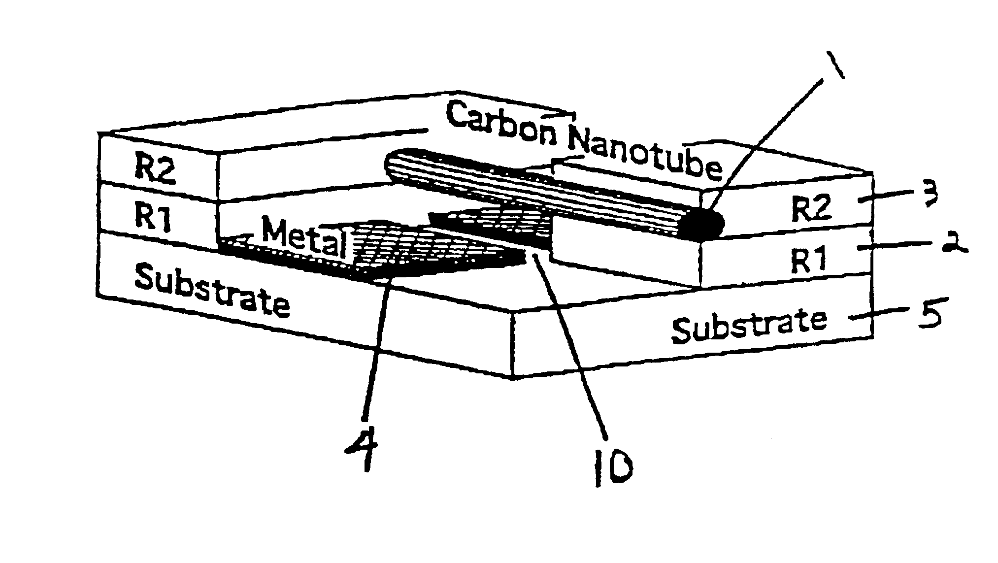
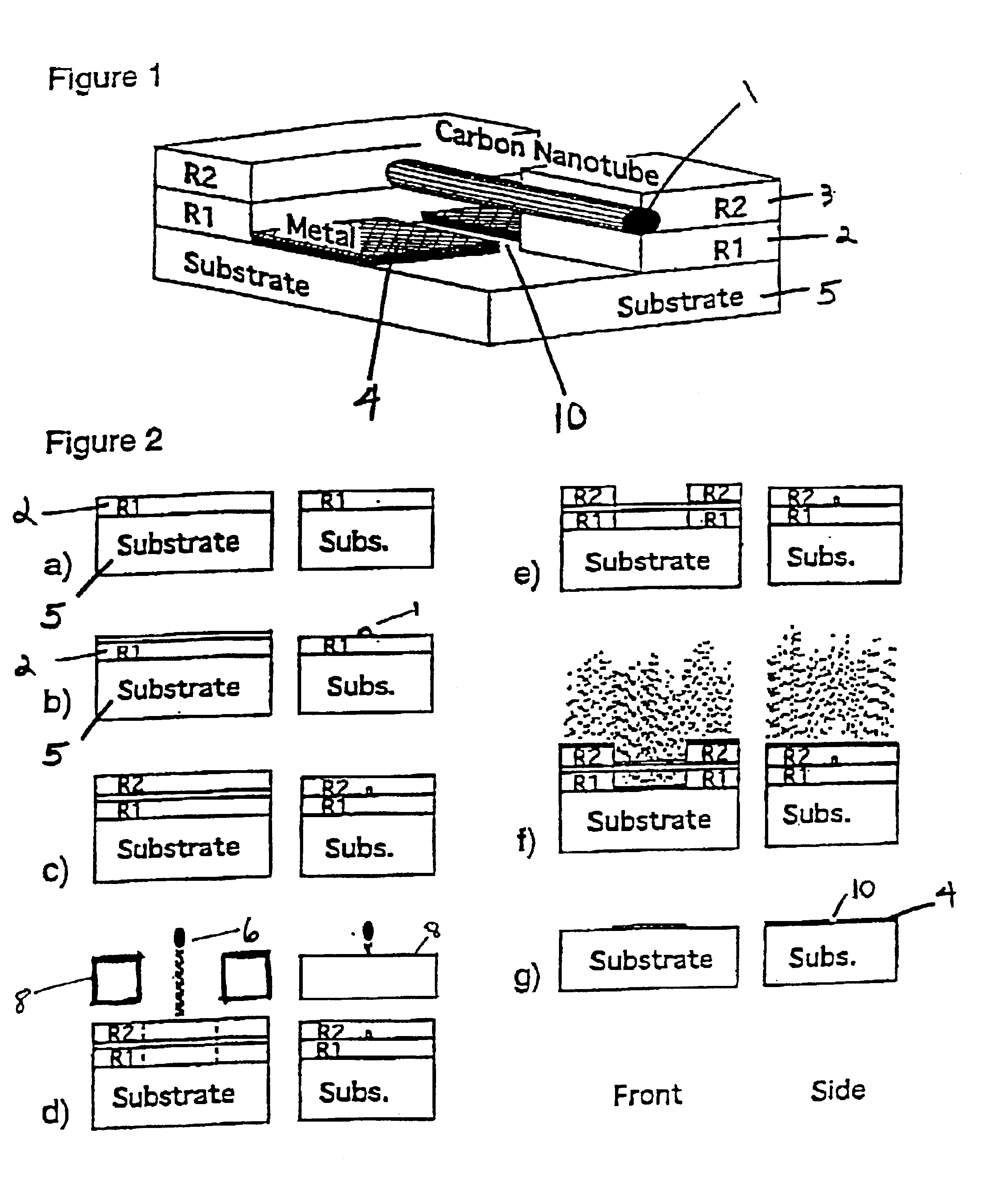
[0021]The present invention is directed to a method of fabricating nanogaps on an electrode. The invention may utilize single-wall nanotubes (SWNTs), or a bundle of SWNTs, or multi-wall “nanotubes” (MWNTs). For simplicity, as used herein, the term nanotube (NT) may refer to an SWNT, an SWNT bundle or an MWNT, all of which can be used for this process. Each of these forms of NTs is better suited for certain tasks. For example, individual SWNTs will provide the narrowest gaps, while the large mechanical rigidity of MWNTs are best for making long gaps. The instant method produces gaps that vary in size from 1 nm to 50 or 100 nm in diameter.

[0022]FIG. 1 shows the profile of the tri-layer system with a partial monolayer of an NT 1 embedded between two layers, shown as first layer 2 and second layer 3. In an embodiment of the invention, the two layers are made of resist material (such as PMMA). However, as mentioned above, there are a variety of two-layer systems that may be used for the ...


PUM

PropertyMeasurementUnit
diameteraaaaaaaaaa
diameteraaaaaaaaaa
diameteraaaaaaaaaa

Abstract

A shadow mask method to fabricate electrodes with nanometer scale separation utilizes nanotubes (NTs). Metal wires with gaps are made by incorporating multi-wall carbon nanotubes (MWNTs) or single-wall carbon nanotubes (SWNTs) (or bundles thereof) into a tri-layer electron beam lithography process. The simple, highly controllable, and scaleable method can be used to make gaps with widths between 1 and 100 nm. Electronic transport measurements performed on individual SWNTs bridge nanogaps smaller than 30 nm. Metallic SWNTs exhibit quantum dot behavior with an 80 meV charging energy and a 20 meV energy level splitting. Semiconducting SWNTs show an anomalous field effect transistor behavior.

Description

[0001]This application claims the benefit of U.S. Provisional application No. 60 / 167,851 filed Nov. 29, 1999.FIELD OF THE INVENTION[0002]The present invention relates to providing a molecular electronic device by fabricating nanogaps on an electrode.BACKGROUND OF THE INVENTION[0003]The rising interest in electrical properties of single molecules is triggered by physical properties that emerge at the transition between the atomic and the bulk scales. Moreover, there is a strong possibility that building blocks of future electronic devices will be found in such systems. One key challenge is attaching probes to nanometer size objects. Early methods to produce nanometer-size gaps (“nanogaps”) were complex and provided a low yield. These include standard electron-beam (e-beam) lithography, break junctions, carbon nanorods, electrochemical growth, and electromigration.[0004]As commercial integrated circuit design rules begin to incorporate sub-100 nm critical dimensions, the possibility o...

Claims


Application Information

Patent Timeline
Patent Type & Authority Patents(United States)
IPC IPC(8): H01L21/02H01L21/033H01L51/40H01L21/3213H01L51/05H01L51/30H01L51/00
CPCB82Y10/00H01L21/0334H01L21/32139H01L51/0021Y10S977/75H01L51/0048H01L51/0052Y10S977/752H10K71/60H10K85/221H10K85/615
Inventor JOHNSON, JR., ALAN T.RADOSAVLJEVIC, MARKOLEFEBVRE, JACQUES
Owner THE TRUSTEES OF THE UNIV OF PENNSYLVANIA
Why Eureka
Try Eureka