Digital video-processing unit
- Summary
- Abstract
- Description
- Claims
- Application Information
AI Technical Summary
Benefits of technology
Problems solved by technology
Method used
Image
Examples
first embodiment
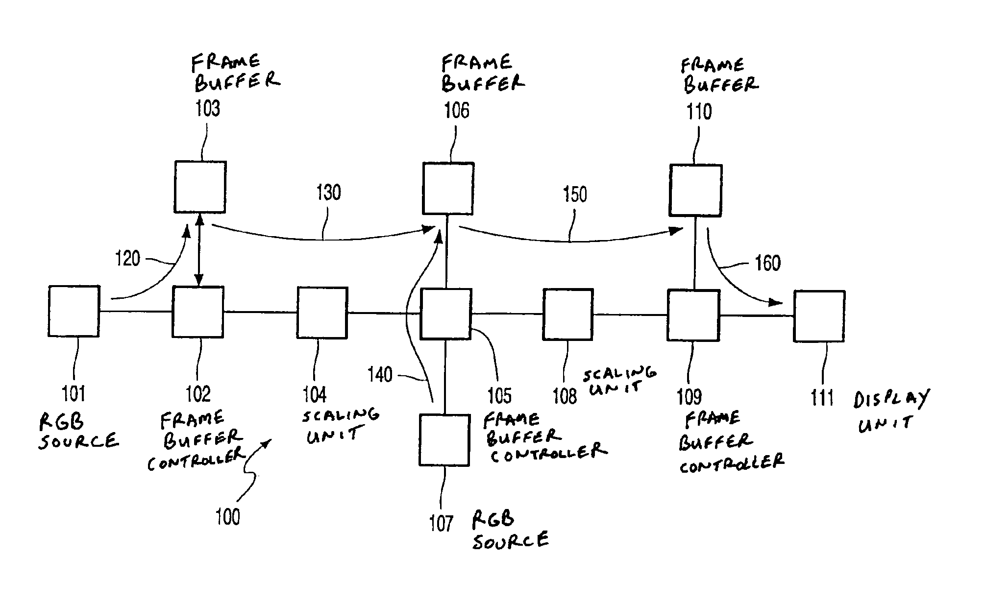
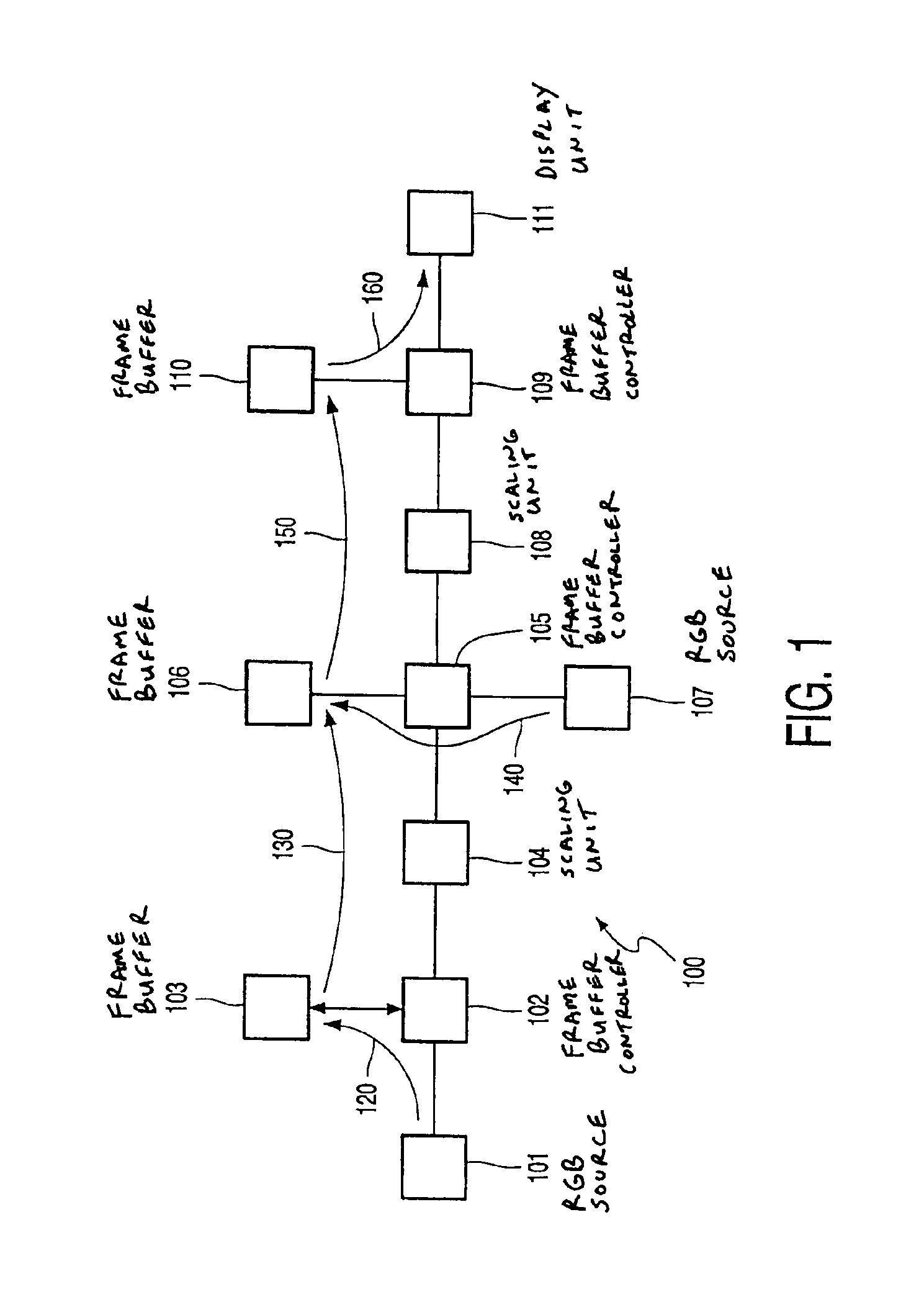
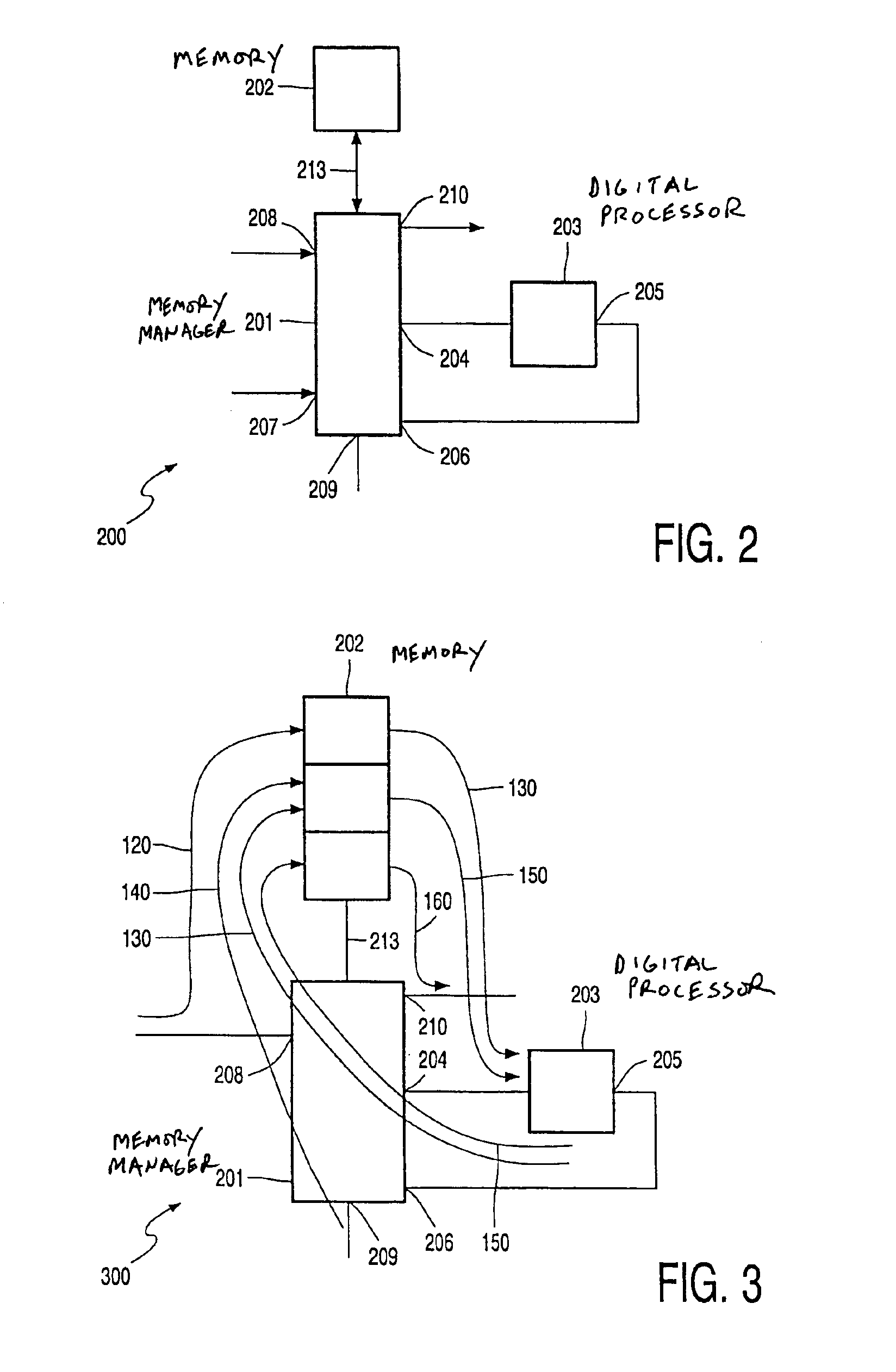
[0031]FIG. 2 shows a block diagram 200 of the architecture of the video-processing unit in accordance with the invention. The digital video-processing unit comprises processing means 203, for example, a digital processor for processing an input signal to an output data signal, memory means 202, for example, a video memory for storing said input signal prior to supply to said digital processor and for storing said output signal after processing in the digital processor 203, and a video memory manager 201 coupled to the digital processor 203 and the video memory 202. An output of the digital processor is coupled to an input of the video memory manager 201, and the video memory manager is further arranged to transfer the output data signal from the digital processor 213 to the video memory 202 for storing the output data signal, and to transmit the output data signal from the video memory 202 to the output device 111. Furthermore, the video memory manager 201 may have, for example two ...
second embodiment
[0033]FIG. 3 shows a process diagram indicating the processes running in time multiplex in the digital video-processing unit 300 with the new architecture. Each of the processes I to V, listed above, is represented in the process diagram by an arrow and the corresponding number as indicated in FIG. 1. In order to reduce the size of the video memory 202, the first and third frame buffers 103, 110 of the architecture indicated in the block diagram of FIG. 1 are realized as cyclic memory buffers in the invention. A minimum memory size is advantageous for integration of a memory, for example SDRAM, in a single chip design of the video-processing unit.
[0034]The cyclic frame buffers store only a part of a complete image, for example several, (5 or 10) lines of the complete image or frame. When the first and third frame buffers 103, 110 comprise cyclic frame buffers, the different processes I to V running on the digital video-processing unit require proper scheduling. For example, process ...
third embodiment
[0035]In order to reduce the bandwidth of the memory 202, processes I and II do not necessarily need to process all pixels of one frame every field. To this end, in the invention, processes I and II can update the complete image as is stored in the second frame buffer 106 in a period covering several frame times, for example, in the odd field, only the left half of the image of the screen can be processed, and the right half of the screen can be processed in the even field. In this way, the total bandwidth of the video memory 202, i.e. the sum of the bandwidths of the first, second and third frame buffers 103, 106, 110 of the different processes, is reduced. However, when this reduced bandwidth is applied, frame tearing may be introduced. Furthermore, the bandwidth of the third frame buffer 110 of process V cannot be reduced, because no continuous data stream can then be sent to the display unit 111, which data stream is related to a predetermined output clock frequency of the displ...
PUM
 Abstract
Description
Claims
Application Information


