Deep wordline trench to shield cross coupling between adjacent cells for scaled NAND

a cross coupling and trench technology, applied in the field of flash memory, can solve the problems of limiting the number of states, affecting the operation of the device, so as to reduce the effect of disturbs and yupin effect errors

Inactive Publication Date: 2005-05-24
SANDISK TECH LLC
View PDF58 Cites 126 Cited by
  • Summary
  • Abstract
  • Description
  • Claims
  • Application Information

AI Technical Summary

Benefits of technology

[0009]The present invention is an improved structure for high density NAND type flash memory that minimizes the effect of disturbs and Yupin effect errors.
[0011]Another aspect of the invention is a flash memory device formed from a substrate. The device comprises strings of adjacent transistors of a NAND architecture comprising a first select gate, a plurality of floating gates, and a second select gate, the plurality of floating gates formed above the substrate, wherein the strings are separated by shallow trench isolation areas. The device has two or more discrete programming levels programmed by increasing a programming potential until the levels are reached, wherein once the floating gates have reached a steady state a linear increase in programming potential results in an approximately linear increase in floating gate charge given a constant potential surrounding environment. Wordlines extend across adjacent strings and between the floating gates into the shallow trench isolation areas, such that when a floating gate of a selected string is read or verified, the wordline minimizes deviation from the linear increase due to voltage variations in the surrounding environment.

Problems solved by technology

One type of error is termed a “disturb,” wherein electrons are unintentionally added to or taken away from a floating gate during operation of the memory.
One source of a disturb is the presence of a leaky oxide dielectric positioned between the floating gate and another conductive gate of a cell.
The charge level programmed onto a floating gate of a cell changes when such a leaky oxide is present, thus leading to the possibility that the state of the cell will be incorrectly read if the change in charge has been large enough.
This necessarily limits the number of states that can be included in a multi-state flash EEPROM system since the total available voltage range is limited.
Any potential present in an adjacent cell or string may influence the reading of a selected cell, including those in the channel, floating gate, or control gates etc. . . . Such interference from the subsequently programmed neighbor cell distorts the voltages of the selected cell, possibly leading to an erroneous identification of its memory state during reading.

Method used


Image

  • Deep wordline trench to shield cross coupling between adjacent cells for scaled NAND
  • Deep wordline trench to shield cross coupling between adjacent cells for scaled NAND
  • Deep wordline trench to shield cross coupling between adjacent cells for scaled NAND

Examples


Embodiment Construction

[0025]The following is a detailed description of illustrative embodiments of the present invention. As these embodiments of the present invention are described with reference to the aforementioned drawings, various modifications or adaptations of the methods and or specific structures described may become apparent to those skilled in the art. All such modifications, adaptations, or variations that rely upon the teachings of the present invention, and through which these teachings have advanced the art, are considered to be within the scope of the present invention. Hence, these descriptions and drawings are not to be considered in a limiting sense, as it is understood that the present invention is in no way limited to the embodiments illustrated.

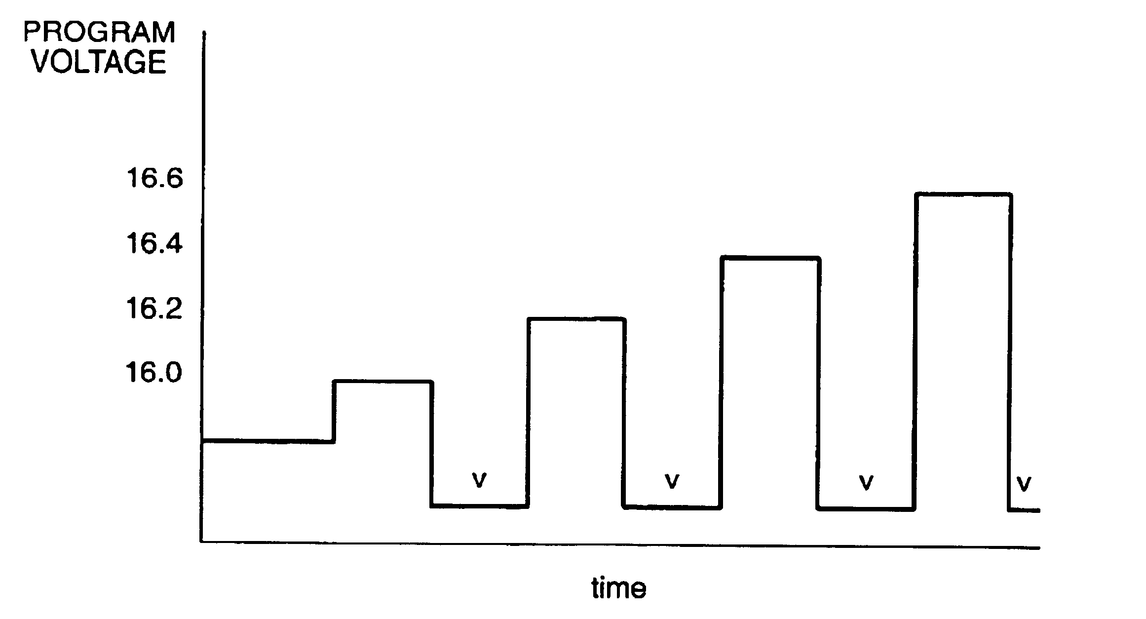
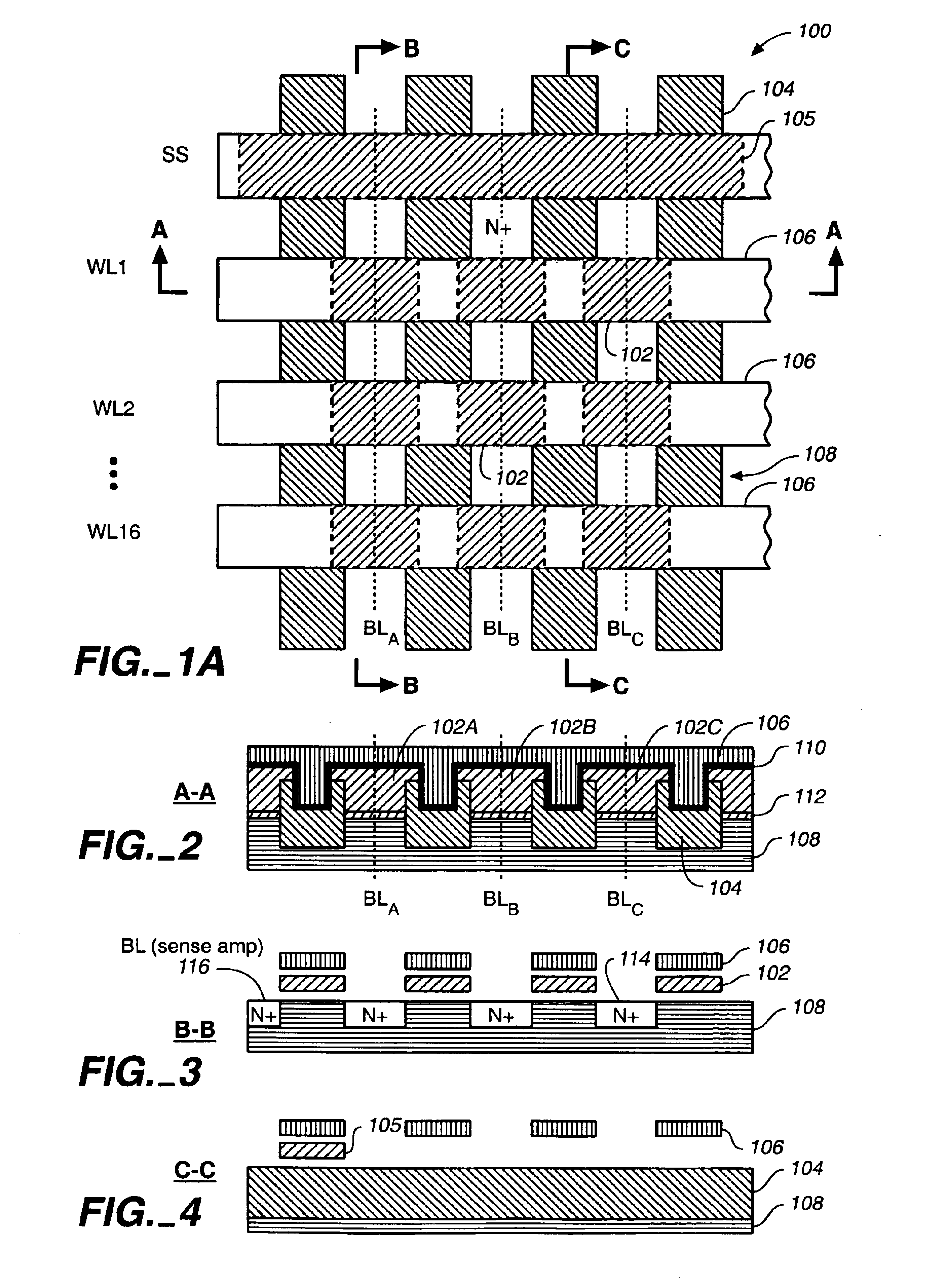
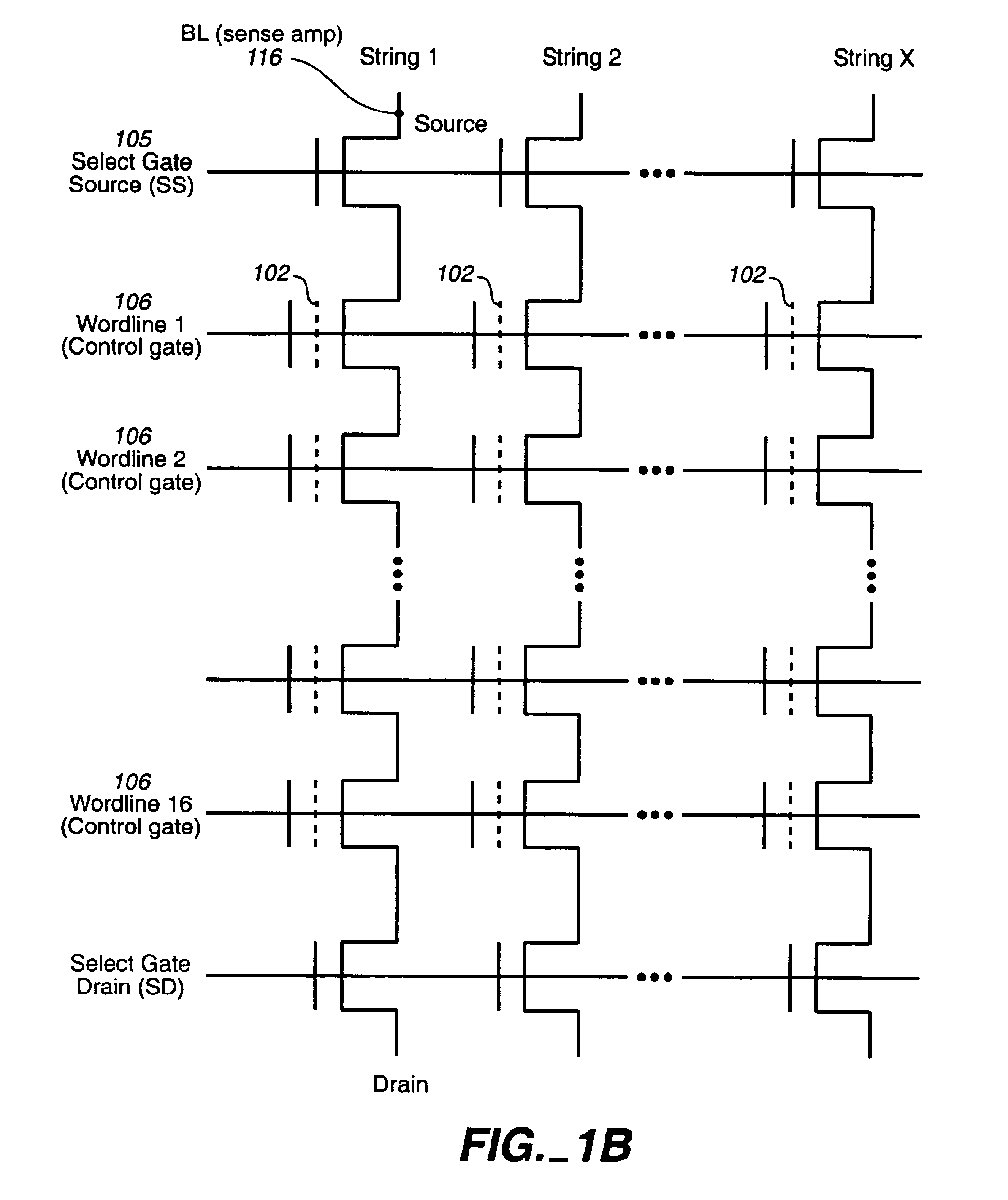
[0026]FIG. 1A illustrates a plan view of an embodiment of the NAND flash memory of the present invention. FIGS. 2-4 are cross sections taken through the structure shown in FIG. 1A. An electrical equivalent circuit of the memory array is give...


PUM


Abstract

A NAND flash memory structure with a wordline or control gate that provides shielding from Yupin effect errors and generally from potentials in adjacent strings undergoing programming operations with significant variations in potential.

Description

CROSS REFERENCE TO RELATED APPLICATIONS[0001]This application is a continuation-in-part of U.S. patent application Ser. No. 10 / 175,764, filed Jun. 19, 2002. This application is also related to U.S. Pat. No. 5,867,429 entitled “High Density Non-Volatile Flash Memory Without Adverse Effects of Electric Field Coupling Between Adjacent Floating Gates” which is hereby incorporated by this reference in its entirety.BACKGROUND OF THE INVENTION[0002]1. Field of the Invention[0003]This invention relates generally to flash electrically erasable and programmable read only memory (EEPROMS), and more specifically to NAND flash memory with a high memory cell density.[0004]2. Related Art[0005]Most existing commercial flash EEPROM products operate each memory cell with two ranges of threshold voltages, one above and the other below a breakpoint level, thereby defining two programmed states. One bit of data is thus stored in each cell, a 0 when programmed into one state and a 1 when programmed into ...

Claims


Application Information

Patent Timeline
Patent Type & Authority Patents(United States)
IPC IPC(8): G11C16/04G11C11/34H01L21/8247H01L27/115H01L29/788H01L29/792
CPCH01L27/11524H01L27/11521H01L27/115G11C16/0483H10B69/00H10B41/30H10B41/35
Inventor CHIEN, HENRYFONG, YUPIN
Owner SANDISK TECH LLC
Why Eureka
Try Eureka