
Multilayer dielectric tunnel barrier used in magnetic tunnel junction devices, and its method of fabrication

a tunnel junction device and multi-layer dielectric technology, applied in the field of multi-layer dielectric tunnel junction devices used in magnetic tunnel junction devices, can solve the problems of reducing the magnetoresistance ratio of interfaces, oxidation process creating anomalous effects, and difficult to consistently produce devices with nearly the same resistance over typical substrate sizes currently used, etc., to achieve good deposition conformality, reduce or eliminate pinhole formation and breakdown areas, and reduce resistance

Inactive Publication Date: 2005-05-31
MICRON TECH INC
View PDF4 Cites 41 Cited by
  • Summary
  • Abstract
  • Description
  • Claims
  • Application Information

AI Technical Summary

Benefits of technology

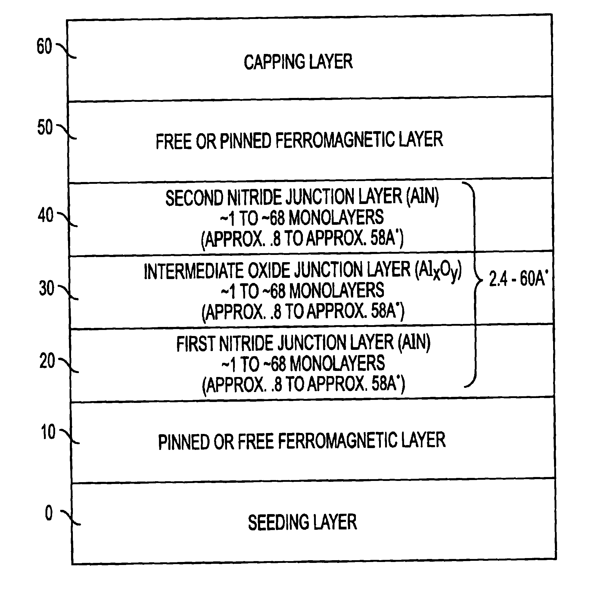
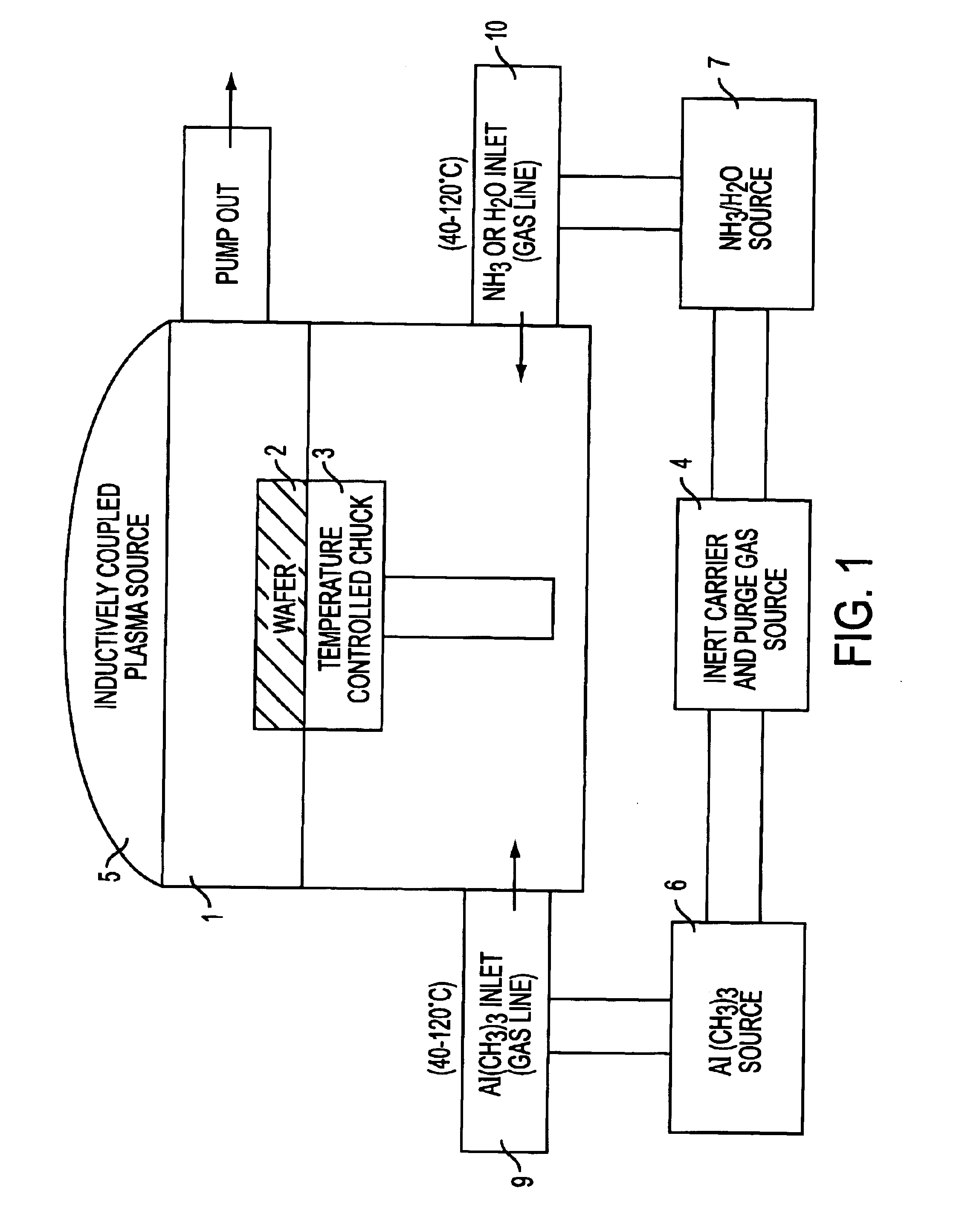
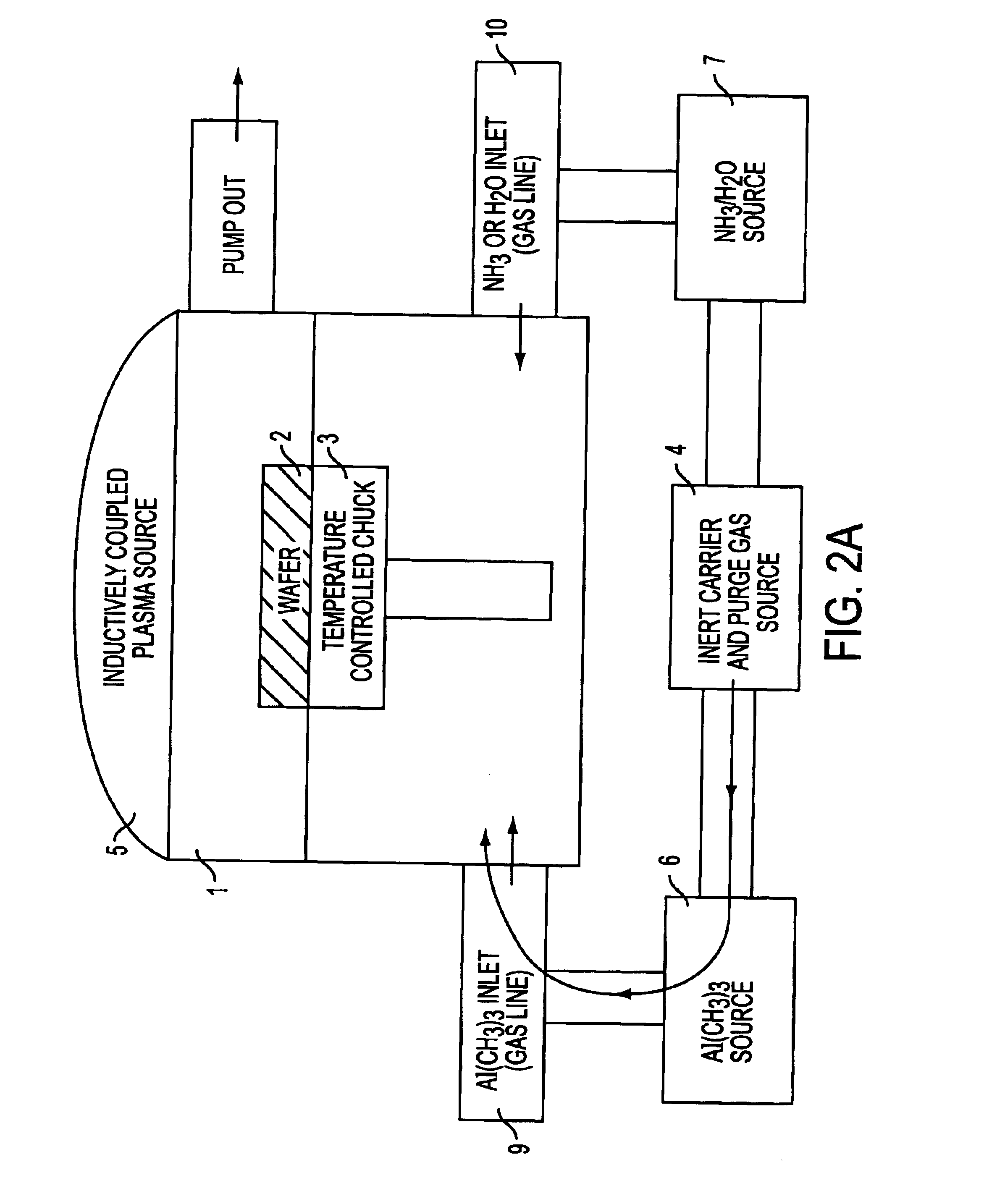
[0012]The present invention provides an ALD deposited multilayer dielectric tunnel barrier film for use in magnetic tunnel junction devices, and a method of fabrication therefor. The tunnel barrier film has reduced resistance and good deposition conformality. An ALD deposited tunnel barrier film, in accordance with the invention, is formed of alternating layers of sequence with plasma or thermal densification steps, to create controlled resistance tunnel barrier layers, which reduce or eliminate pinhole formation and breakdown areas in the films.
[0013]The method aspect of the invention comprises providing an oxide layer, on a first nitride layer, and a second nitride layer on the oxide insulation area. The first nitride layer is disposed on a semiconductor substrate containing a first ferromagnetic film. While the second nitride layer interfaces with a second ferromagnetic film. By conducting the formation of the multilayer dielectric tunnel barrier through atomic layer deposition reactions coupled with thermal anneals, plasma processing, and densification techniques; a highly improved and controlled multilayer tunnel barrier can be achieved which provides a higher breakdown point, lower pinhole occurrences, and good tunneling characteristics for magnetic tunnel junctions.
[0014]The enhanced multilayer tunnel barrier structure is produced by alternating layers of nitride i.e., AlN, and oxide i.e., AlxOy, through atomic layer deposition reactions. The atomic layer deposition reactions allow precise control over the thickness of the alternating layers of nitride and oxide. The thickness of these alternating nitride and oxide layers can be utilized to change the final magnetoresistance of the barrier or barrier height, and reduce the chances of pinhole formation. Furthermore, utilizing ALD processes allows formation of the tunnel barrier structure to occur at temperatures below 300° C., ensuring stability of the alternating layers.
[0015]Therefore, the present invention provides a multilayer dielectric tunnel barrier that has a substantially reduced overall resistance than that associated with conventional structures and methods, while permitting precise tailoring of the thicknesses of the various layers in the tunnel barrier structure. The present invention also provides for memory devices which have reduced pinholing; improved magnetic characteristics, by reducing the occurrence of oxidation of the ferromagnetic materials on either side of the barrier; and anatomically smooth tunnel barrier layer interfaces.

Problems solved by technology

This strong dependence on thickness makes it difficult to consistently produce devices with nearly the same resistance over typical substrate sizes currently used in memory manufacturing processes.
However, the oxidation process creates anomalous effects.
In addition, roughness at the tunnel barrier interfaces lowers the magnetoresistance ratio dramatically, due to partial shorts or tunneling hot spots.
Thus, producing a magnetic tunnel junction material with good resistance uniformity over an entire wafer is challenging.
Another problem arises when the magnetic tunnel junction material is exposed to temperatures greater than 300° C. The magnetoresistance ratio begins to degrade at 300° C. and drops off sharply at 400° C. as a result of increasing resistance.
In addition, as bit sizes are reduced, a challenge arises in producing magnetic tunnel junction material with very low resistance-area products.

Method used


Image

  • Multilayer dielectric tunnel barrier used in magnetic tunnel junction devices, and its method of fabrication
  • Multilayer dielectric tunnel barrier used in magnetic tunnel junction devices, and its method of fabrication
  • Multilayer dielectric tunnel barrier used in magnetic tunnel junction devices, and its method of fabrication

Examples


Embodiment Construction

[0036]The present invention will be understood from the following detailed discussion of the exemplary embodiments which is presented in connection with the accompanying drawings.

[0037]The present invention provides a multilayer dielectric tunnel barrier used in magnetic tunnel junction devices and its method of fabrication. The multilayer film has lower barrier layer resistance, is very conformal, and can be made as a thicker or thinner film with fewer pinholes.

[0038]In the following description, specific details such as layer thicknesses, process sequences, and material compositions are set forth to provide a complete understanding of the present invention. However, it will be obvious to one skilled in the art that the present invention can be employed without using such specific details. In addition, in order for a simplified description, techniques, processes, and equipment that are well-known in the art have not been described in detail.

[0039]For purposes of the present inventi...


PUM

PropertyMeasurementUnit
temperaturesaaaaaaaaaa
temperatureaaaaaaaaaa

Abstract

A multilayer dielectric tunnel barrier structure and a method for its formation which may be used in non-volatile magnetic memory elements comprises an ALD deposited first nitride junction layer formed from one or more nitride monolayers i.e., AlN, an ALD deposited intermediate oxide junction layer formed from one or more oxide monolayers i.e., AlxOy, disposed on the first nitride junction layer, and an ALD deposited second nitride junction layer formed from one or more nitride monolayers i.e., AlN, disposed on top of the intermediate oxide junction layer. The multilayer tunnel barrier structure is formed by using atomic layer deposition techniques to provide improved tunneling characteristics while also providing anatomically smooth barrier interfaces.

Description

CROSS-REFERENCE TO RELATED APPLICATIONS[0001]The present application is a divisional application of U.S. Pat. application Ser. No. 10 / 165,301, filed on Jun. 10, 2002, the disclosure of which is herewith incorporated by reference in its entirety.BACKGROUND OF THE INVENTION[0002]1. Field of the Invention[0003]This invention relates generally to the field of semiconductor memory, sensor applications and logic devices. The invention relates more specifically to a multilayer dielectric tunnel barrier used in magnetic tunnel junction devices, and its method of fabrication.[0004]2. Description of the Related Art[0005]Recently, magnetoresistive random access memory (MRAM) devices have been developed as possible use for data storage. The nonvolatility, fast access times, and less complex structure of MRAM offers some advantages over DRAM and FLASH memory devices.[0006]The two most critical layers in an MRAM memory cell are the tunnel barrier, which is often formed with AlxOy i.e., Al2O3, and...

Claims


Application Information

Patent Timeline
Patent Type & Authority Patents(United States)
IPC IPC(8): C23C16/30C23C16/40H01F41/00H01F41/22H01F10/00H01F41/32H01F41/14H01F10/32H01L21/02H01L21/316C23C16/44C23C16/455H01L43/12
CPCB82Y25/00C23C16/303C23C16/403C23C16/45529H01F10/3254H01L43/12H01F41/32H01L21/02178H01L21/0228H01L21/3162H01F41/22H01L21/31683H10N50/01
Inventor DREWES, JOEL A.
Owner MICRON TECH INC
Learn More