Stacked IC

Inactive Publication Date: 2005-05-31
RAMTEK TECH
View PDF2 Cites 126 Cited by
  • Summary
  • Abstract
  • Description
  • Claims
  • Application Information

AI Technical Summary

Benefits of technology

[0006]It is an object of the present invention to provide a stacked IC with a plurality of p

Problems solved by technology

Although the manner for fabricating this stacked IC 1 is cost effective, the internal structure of the second IC package unit 12 may be damaged during the operation of bending the lead wires 112.
In addition, such manner is time-consuming.
However, t

Method used


Image

  • Stacked IC
  • Stacked IC
  • Stacked IC

Examples


first embodiment

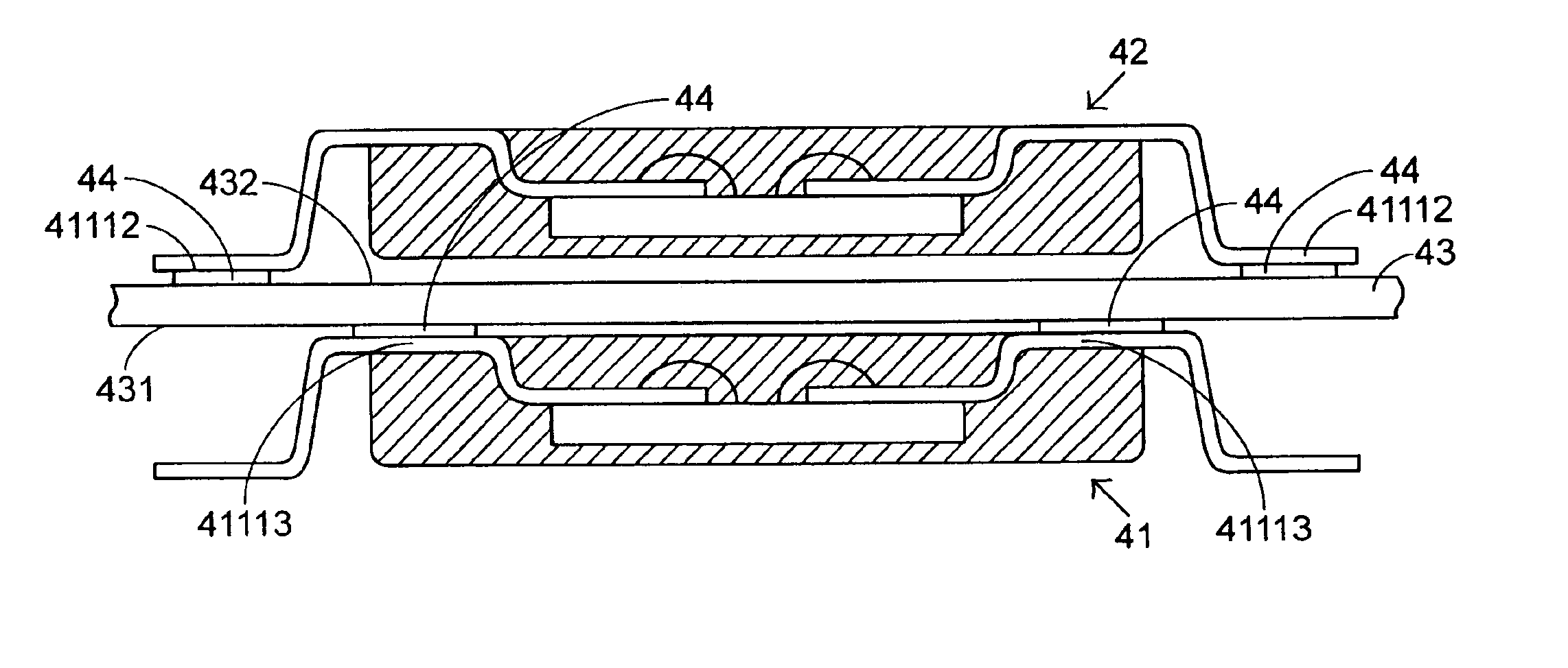
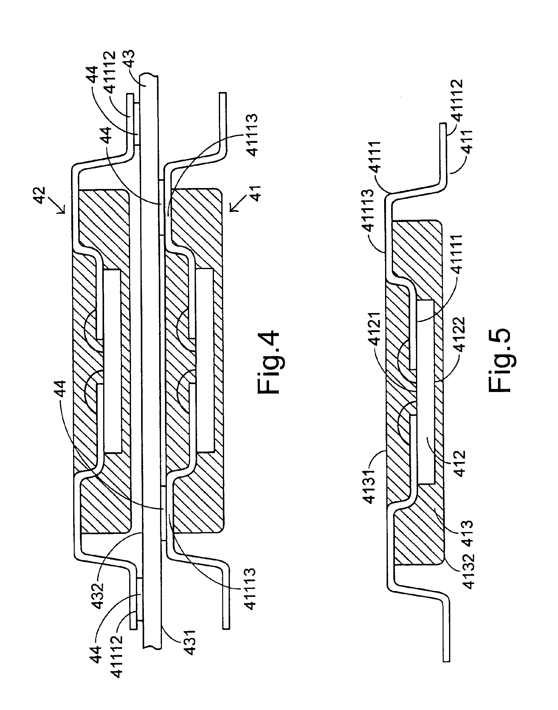
[0031]Referring to FIG. 4, a schematic view of a stacked IC according to the present invention is shown. The stacked IC comprises a first IC package unit 41, a second IC package unit 42 and an interface layer 43. The first IC package unit 41 and the second IC package unit 42 have the same structure and are provided on the bottom and the top of the stacked IC, respectively. The interface layer 43 is sandwiched between the first IC package unit 41 and the second IC package unit 42. Through the interface layer 43, the first IC package unit 41 and the second IC package unit 42 are electrically connected with each other.

[0032]Please refer to FIG. 5. Take the first IC package unit 41 for example. The first IC package unit 41 comprises a lead frame 411, an IC chip 412 and an encapsulant resin 413. The IC chip 412 has a first surface 4121 and a second surface opposite to each other. The first surface 4121 of the IC chip 412 has thereon a plurality of electrical pads (not shown). The lead fr...

fourth embodiment

[0039]Referring to FIG. 10, a schematic view of a stacked IC according to the present invention is shown. This stacked IC is similar to that of FIG. 4, except that the second IC package unit 42 arranged on the top is replaced by a thin small out-line package (TSOP) unit 62. The lead wire 621 of the TSOP unit 62 is bonded to the solder pads on the top of the interface layer 43 so as to make electrical connection of the first IC package unit 41 and the TSOP unit 62.

[0040]Likewise, as shown in FIG. 11, the stacked IC is similar to that of FIG. 4, except that the second IC package unit 42 arranged on the top is replaced by a ball grid array (BGA) package unit 72. The solder ball 721 of the BGA package unit 72 is bonded to the solder pads on the top of the interface layer 43 so as to make electrical connection of the first IC package unit 41 and the BGA package unit 72.

[0041]The present invention is illustrated by referring to a stacked IC with two stacked memory chips such as DRAM, DDR ...


PUM


Abstract

A stacked IC includes a first IC package unit, a second IC package unit and an interface layer. The first IC package unit includes an IC chip, an encapsulant resin and a plurality of lead wires. The IC chip is encapsulated by the encapsulant resin. Each of the lead wires includes a first end connected to the IC chip and encapsulated by the encapsulant resin, a second end extending outside the encapsulant resin, and a bend portion arranged between the first end and the second end and having at least one surface exposed outside of the encapsulant resin. The second IC package unit has the same structure as the first IC package unit. The interface layer is sandwiched between the first IC package unit and the second IC package unit, and has a first side connected to the bend portion of the first IC package unit and a second side connected to the second end of the second IC package unit.

Description

FIELD OF THE INVENTION[0001]The present invention relates to a stacked IC, and more particularly to a stacked IC with a plurality of package units in a stack form.BACKGROUND OF THE INVENTION[0002]With the rapid progress of semiconductor industries, the integrated circuits (ICs) used in electronic devices are developed toward minimization. high operating speed and increasing integration level. In a computer system or similar electronic products, CPU determines system performance, and the capacity and the operating speeds of the memory chips are important factors that affect data processing efficiency. Take a memory chip for example. Nowadays, for complying with a requirement of miniaturization, the memory chip is designed to have a high storage capacity with a reduced size. For a purpose of reducing cost and size, a so-called stacking method is widely used to interconnect multiple memory chips in a stack form so as to form a memory module, i.e. a stacked IC.[0003]Referring to FIG. 1,...

Claims


Application Information

Patent Timeline
IPC IPC(8): H01L23/495H01L23/48H01L25/10H05K1/14
CPCH01L23/4951H05K1/141H01L25/105H01L2225/107H01L2224/48091H01L2224/48247H01L2224/4826H01L2924/01078H01L2924/14H01L2924/1433H01L2924/15311H05K1/145H05K2201/049H05K2201/10515H05K2201/10689H01L2225/1041H01L24/48H01L2225/1029H01L2924/00014H01L2224/45099H01L2224/45015H01L2924/207
Inventor TSAI, CHENG-HSUN
Owner RAMTEK TECH
Why Eureka
Try Eureka