Thin film piezoelectric element

a piezoelectric element and thin film technology, applied in piezoelectric/electrostrictive device material selection, piezoelectric/electrostrictive/magnetostrictive device material selection, device material selection, etc., can solve the problems of large variations, inability to be neglected, variations and deterioration in characteristics become remarkable, etc., to achieve high piezoelectric characteristic and high piezoelectric characteristic

Inactive Publication Date: 2005-05-31
PANASONIC CORP
View PDF8 Cites 9 Cited by
  • Summary
  • Abstract
  • Description
  • Claims
  • Application Information

AI Technical Summary

Benefits of technology

[0009]The present invention is for solving the above problems and has an object to realize a piezoelectric thin film having a high piezoelectric characteristic even in the thin film, by controlling and optimizing the microscopic crystal structure of a piezoelectric thin film material, and to provide a thin film piezoelectric element which is able to withstand practical use. Also, the present invention has an

Problems solved by technology

However, in piezoelectric materials made by a manufacturing method centering on the sintering method, a conventional manufacturing method, as the thickness thereof is made thin, particularly as the thickness approaches a thickness of about 10 μm, it gets nearer to the size of the crystal grains constituting the materials, and thus the effect of the crystal grains becomes unable to be neglected.
For this reason, there arises a problem that variations and deterioration in the characteristics become remarkable, and therefore, in order to avoid this problem, a method of forming a piezoelectric substance in which a thin film technology or the like are applied as the replacement of the sintering method has been studied in recent years.
However, in piezoelectric thin films formed by these techniques, there are large variations in their characteristics caused by the problems of grain boundary and crystalline orientation, when compared with the piezoelectric characteristics of sintering-formed piezoelectric materials referred to as bulk materials.
Further, due to the effects of stress appl

Method used


Image

  • Thin film piezoelectric element
  • Thin film piezoelectric element

Examples


Embodiment Construction

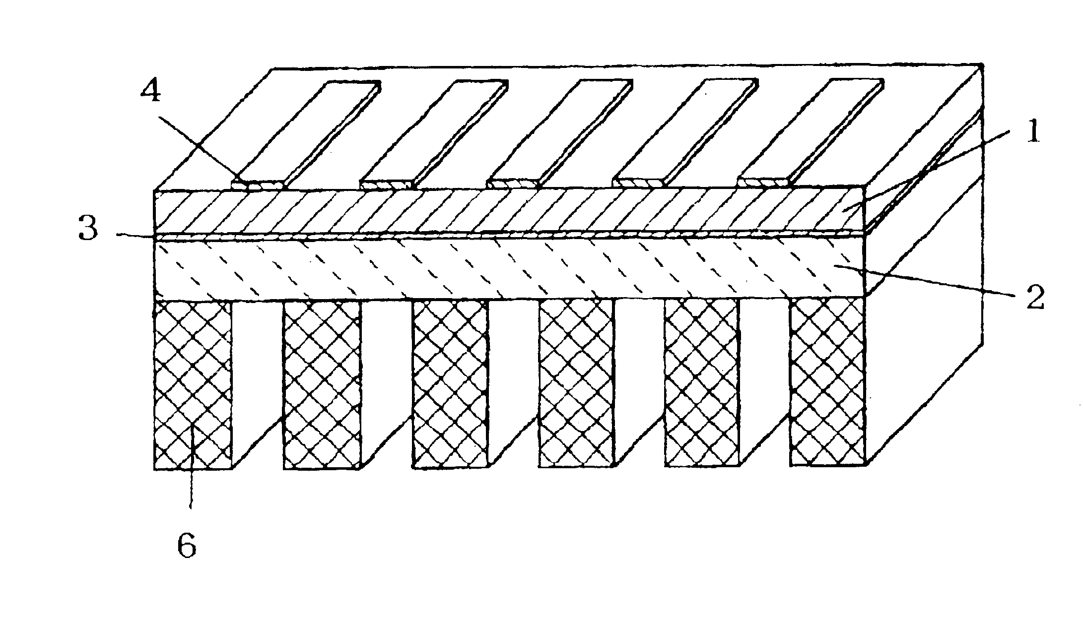
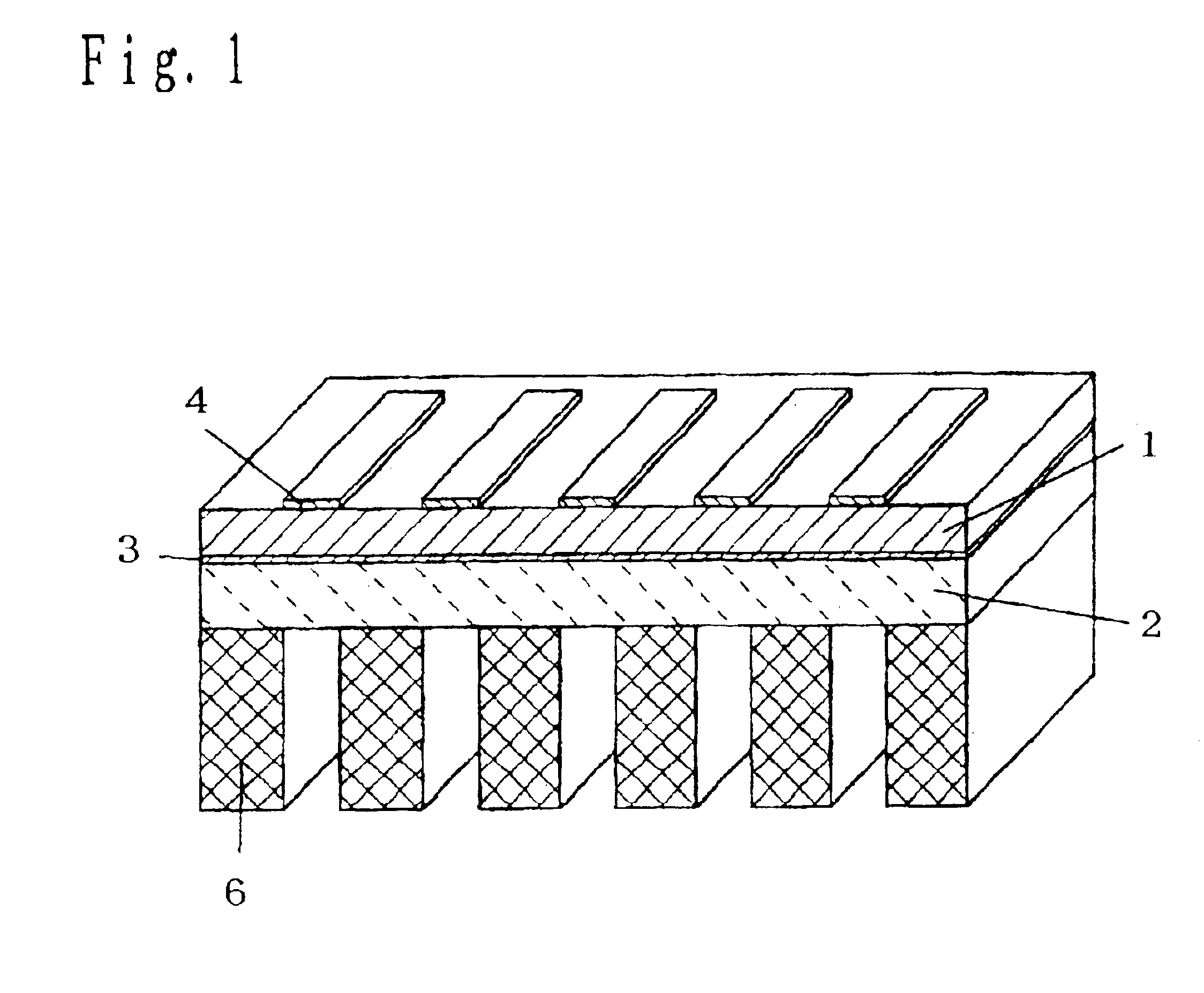
[0019]A configuration of a piezoelectric element according to one embodiment of the invention will be described with reference to a drawing.

[0020]FIG. 1 shows one embodiment of a thin film piezoelectric element according to the invention. A piezoelectric thin film 1 has a composition of Pb(Zr1-xTix)O3 (0.47≦x≦1) (hereinafter, referred to as PZT) and has a film thickness of substantially 3 μm. This film was formed on a substrate 6 of magnesium oxide. Then, the substrate 6 was worked into a diaphragm structure and thus configured such that the piezoelectric thin film 1 can easily vibrate.

[0021]Herein, the piezoelectric thin film 1 was formed by a sputtering method in which a sintered-body target having about the same composition as that of the formed thin film is placed in a vacuum chamber and plasma is generated over the target in a gas of an oxidizing atmosphere, thereby depositing the thin film 1 on the substrate 6 heated.

[0022]The used substrate 6 of magnesium oxide is a single cr...


PUM


Abstract

To provide a piezoelectric thin film having an improved and stable characteristic by controlling stress applied during forming a piezoelectric thin film and providing the piezoelectric thin film having a perovskite structure. A thin film piezoelectric element in which a lower electrode is formed on a substrate, a piezoelectric thin film containing lead is formed on the lower electrode, and an upper electrode is further placed on the piezoelectric thin film, characterized in that the piezoelectric thin film is a dielectric with the perovskite structure having lead, zirconium, and titanium as the main ingredients, and is in a composition region in which, in the composition of the whole piezoelectric thin film, the. Zr/(Zr+Ti) ratio is not less than substantially 0.53, and has a crystal structure of the tetragonal system in which a c axis is longer than an a axis.

Description

[0001]This application is a U.S. National Phase Application of PCT International Application PCT / JP01 / 06318.TECHNICAL FIELD[0002]The present invention relates to a piezoelectric element using a piezoelectric thin film material.BACKGROUND ART[0003]Generally, a piezoelectric substance is made into different piezoelectric elements according to different kinds of objects, and the elements are widely used as functional electronic components, particularly including an actuator producing deformation by the application of a voltage and a sensor generating a voltage based on the deformation of its element in reverse. As a piezoelectric substance used for the applications of actuators and sensors, Pb-based dielectrics having a large piezoelectric characteristic, particularly perovskite type ferroelectrics of the Pb(Zr1-xTix)O3 family referred to as PZT, have been widely used until now, and they are usually formed by sintering oxides composed of individual elements.[0004]At present, as the tre...

Claims


Application Information

Patent Timeline
IPC IPC(8): H01L41/18H01L41/187H01L41/24H01L41/22H01L41/316
CPCH01L41/316H01L41/1876H10N30/2047H10N30/8554H10N30/076
Inventor KANNO, ISAKUHARA, SHINTAROUNAKANO, TAKANORI
Owner PANASONIC CORP
Why Eureka
Try Eureka