Signal conditioning system with adjustable gain and offset mismatches

a signal conditioning and gain adjustment technology, applied in the field of electronic circuits, can solve problems such as inability to correct for mismatches, significant spurious tones or frequency components at the system output, and affect the signal-to-noise and distortion (sinad) ratio,

a signal conditioning and gain adjustment technology, applied in the field of electronic circuits, can solve problems such as inability to correct for mismatches, significant spurious tones or frequency components at the system output, and affect the signal-to-noise and distortion (sinad) ratio,

US6900750B1Active Publication Date: 2005-05-31ANALOG DEVICES INC

Image

  • Signal conditioning system with adjustable gain and offset mismatches
  • Signal conditioning system with adjustable gain and offset mismatches
  • Signal conditioning system with adjustable gain and offset mismatches

Examples


Embodiment Construction

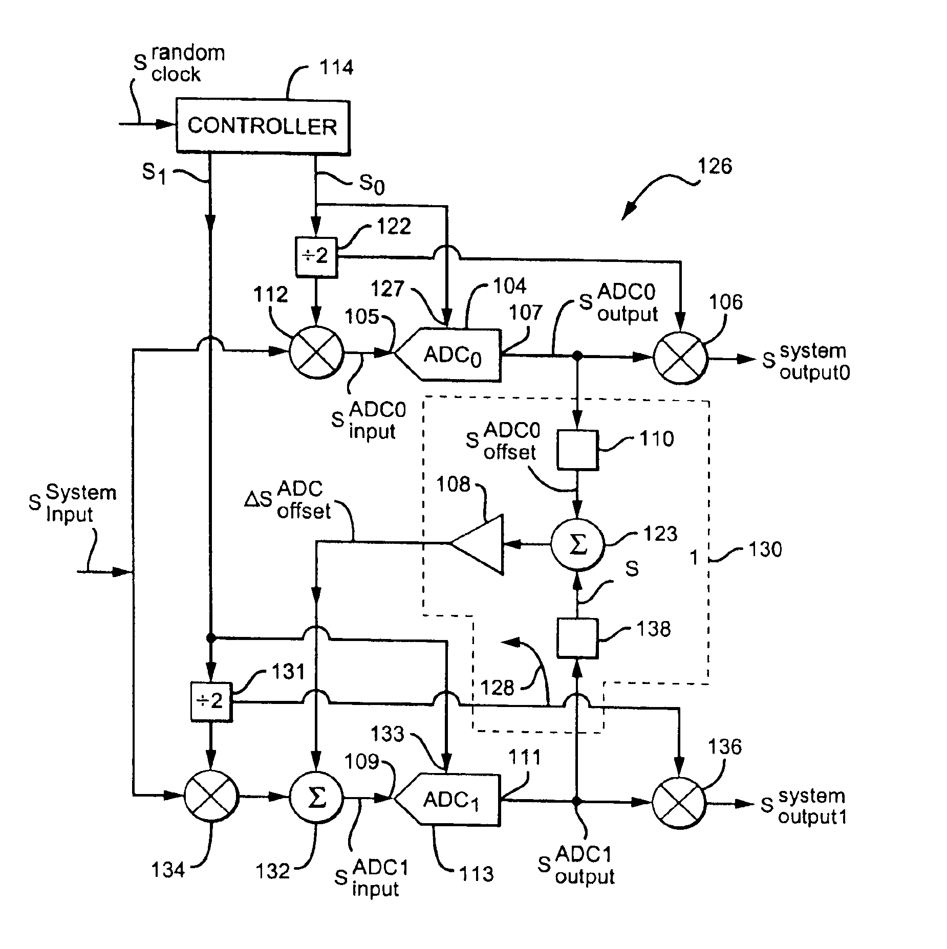
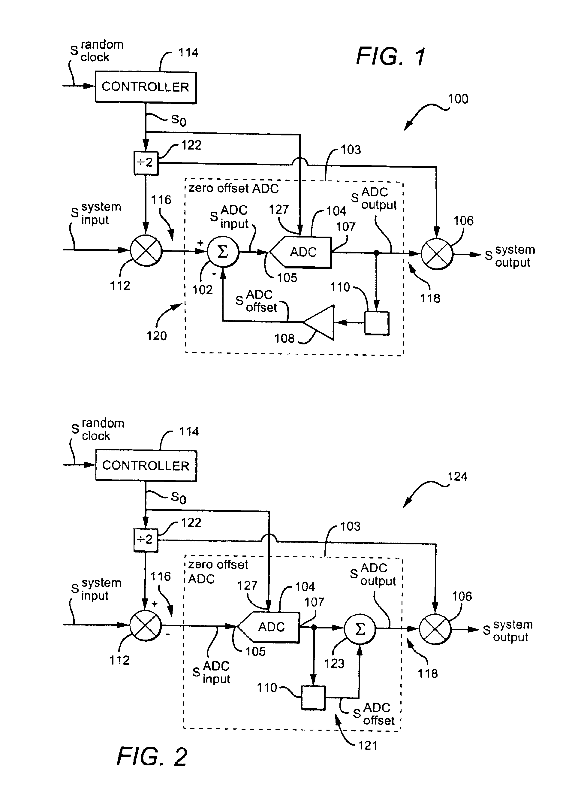
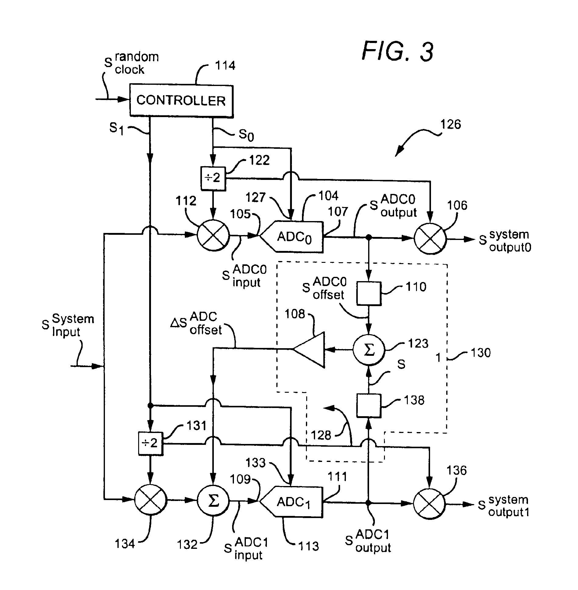
[0040]FIGS. 1-4 and 6-8 illustrate different embodiments of signal conditioning systems in accordance with the present invention. It should be noted that the signal conditioning systems can include, for example, a differential amplifier, an operational amplifier, an analog-to-digital converter (ADC), or a digital to analog converter among others. In the embodiments shown in the following figures, however, the signal conditioning systems include analog-to-digital converters to exemplify the features of the invention.

[0041]FIG. 1 illustrates a signal conditioning system 100 which uses analog techniques to adjust or correct an offset signal. The term “analog techniques” refers to the coupling of an ADC output to an ADC input through a feedback loop in which where the offset signal is subtracted from an analog input signal to condition a digital output signal. It should be noted, however, that the offset signal is subtracted from the analog input signal for simplicity and ease of discus...


PUM


Abstract

A signal conditioning system includes first and second converters coupled to a random clock which provides a random sampling rate. Corresponding offset sensor coupled with the first and second converters sense and adjust an offset signal difference. A gain sensor is coupled with the first and second converters to sense a gain difference between the first and second converters and a gain corrector is coupled with the gain sensor to adjust the gain difference.

Description

BACKGROUND OF THE INVENTION[0001]1. Field of the Invention[0002]This invention relates generally to electronic circuits and, more particularly, to adjusting gain and offset mismatches in signal conditioning systems such as converter circuits.[0003]2. Description of the Related Art[0004]Interleaving is a well-known technique for achieving high sample rates in analog-to-digital converter (ADC) systems. An ADC converts an analog input signal into a digital output signal which represents the analog input signal in digital bits. In a typical implementation, an array of ADCs is arranged to sample the analog input signal in a sequential manner. If each ADC can be clocked at a frequency ƒc and if there are M ADCs, then the maximum effective sampling frequency ƒs for the interleaved system is ƒs=M·ƒc. It is desirable to increase the sampling frequency so that the analog input signal can be resolved more accurately. The resolution depends on the number of bits in the digital output signal use...

Claims


Application Information

Patent Timeline
31 May 2005
Publication
US6900750B1
IPC
H03M1/06; H03M1/12
CPC
H03M1/0621; H03M1/0609; H03M1/1205; H03M1/12
Inventors
NAIRN, DAVID G.