Display and method for driving the same

a technology applied in the field of display and driving method, can solve the problems of unstable discharge, inability to repeatedly stably induce discharge, and saturation of ultraviolet rays with respect, and achieve the effect of improving luminous efficiency

Inactive Publication Date: 2005-05-31
PANASONIC CORP
View PDF21 Cites 80 Cited by
  • Summary
  • Abstract
  • Description
  • Claims
  • Application Information

AI Technical Summary

Benefits of technology

[0024]An object of the present invention is to provide a display device capable of improving the luminous efficiency of all discharge cells which should be turned on and a method of driving the same.
[0025]Another object of the present invention is to provide a display device capable of improving the luminous efficiency of all discharge cells which should be turned on as well as capable of repeatedly stably inducing discharges and a method of driving the same.
[0026]Still another object of the present invention is to provide a display device capable of repeatedly stably inducing discharges even if the lighting rate is changed as well as capable of improving luminous efficiency corresponding to applied power to reduce power consumption and a method of driving the same.

Problems solved by technology

However, ultraviolet rays are saturated with respect to the discharge current.
When the discharge cells are driven at such a low current level that luminance is not saturated, the discharges themselves are unstable.
Consequently, the discharges cannot be repeatedly stably induced.
Accordingly, luminous efficiency cannot be improved with respect to all the discharge cells which should be turned on.
Furthermore, the conventional plasma display device is caused to emit light by supplying a discharge current from the power supply to induce discharges only once.
Accordingly, luminous efficiency is reduced with respect to applied power, resulting in increased power consumption.
Generally, power consumption in the plasma display device is higher than that in the other display device.
When the discharge cells are driven at such a low current level that luminance is not saturated, the discharges themselves are unstable.
When the discharge cells are driven at a low current level, the discharges are made more unstable.

Method used


Image

  • Display and method for driving the same
  • Display and method for driving the same
  • Display and method for driving the same

Examples


first embodiment

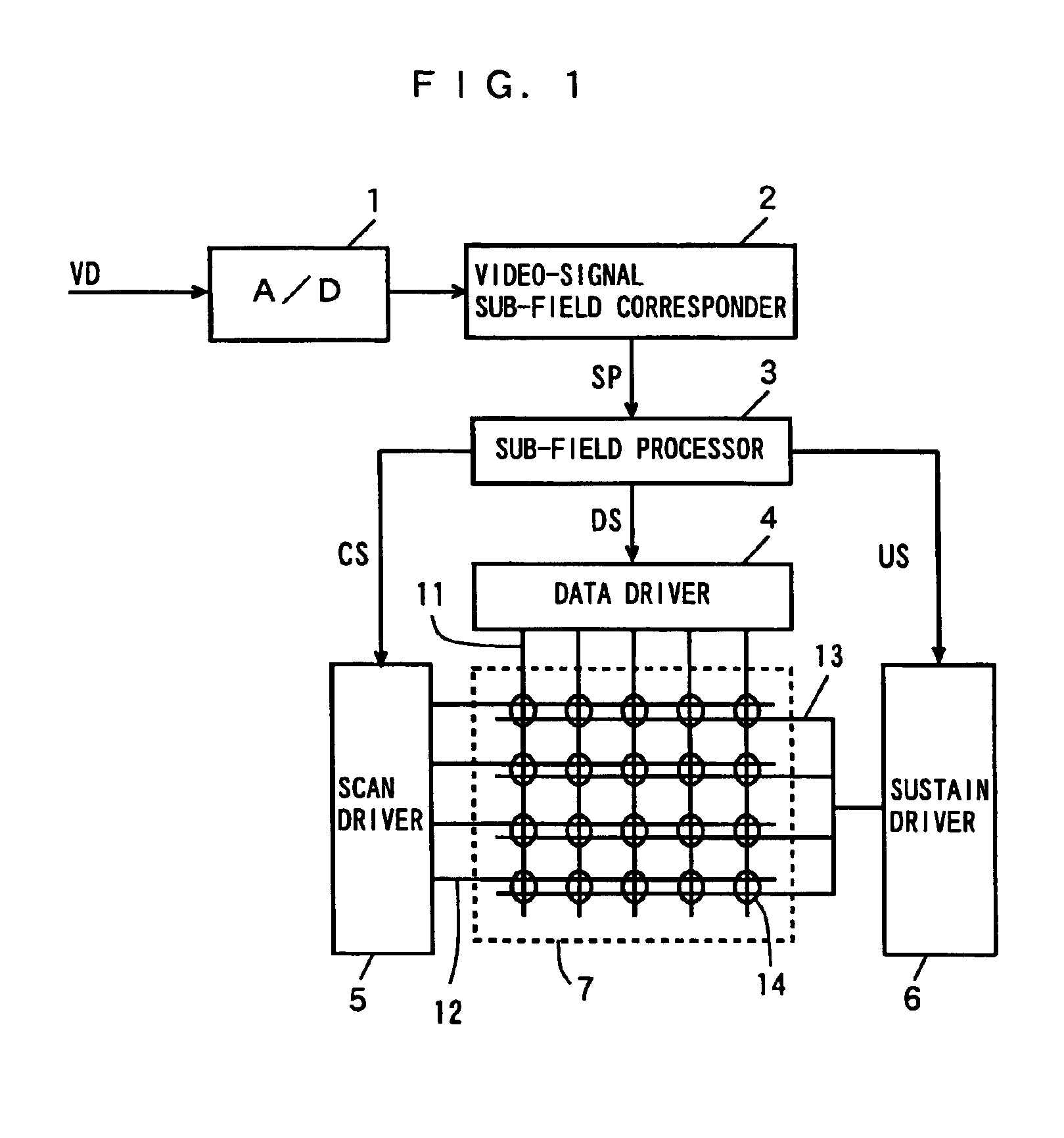
[0165]An AC-type plasma display device will be described as an example of a display device according to the present invention. FIG. 1 is a block diagram showing the configuration of the plasma display device according to the present invention.

[0166]The plasma display device shown in FIG. 1 comprises an A / D converter (an analog-to-digital converter) 1, a video signal / sub-field corresponder 2, a sub-field processor 3, a data driver 4, a scan driver 5, a sustain driver 6, and a PDP (Plasma Display Panel) 7.

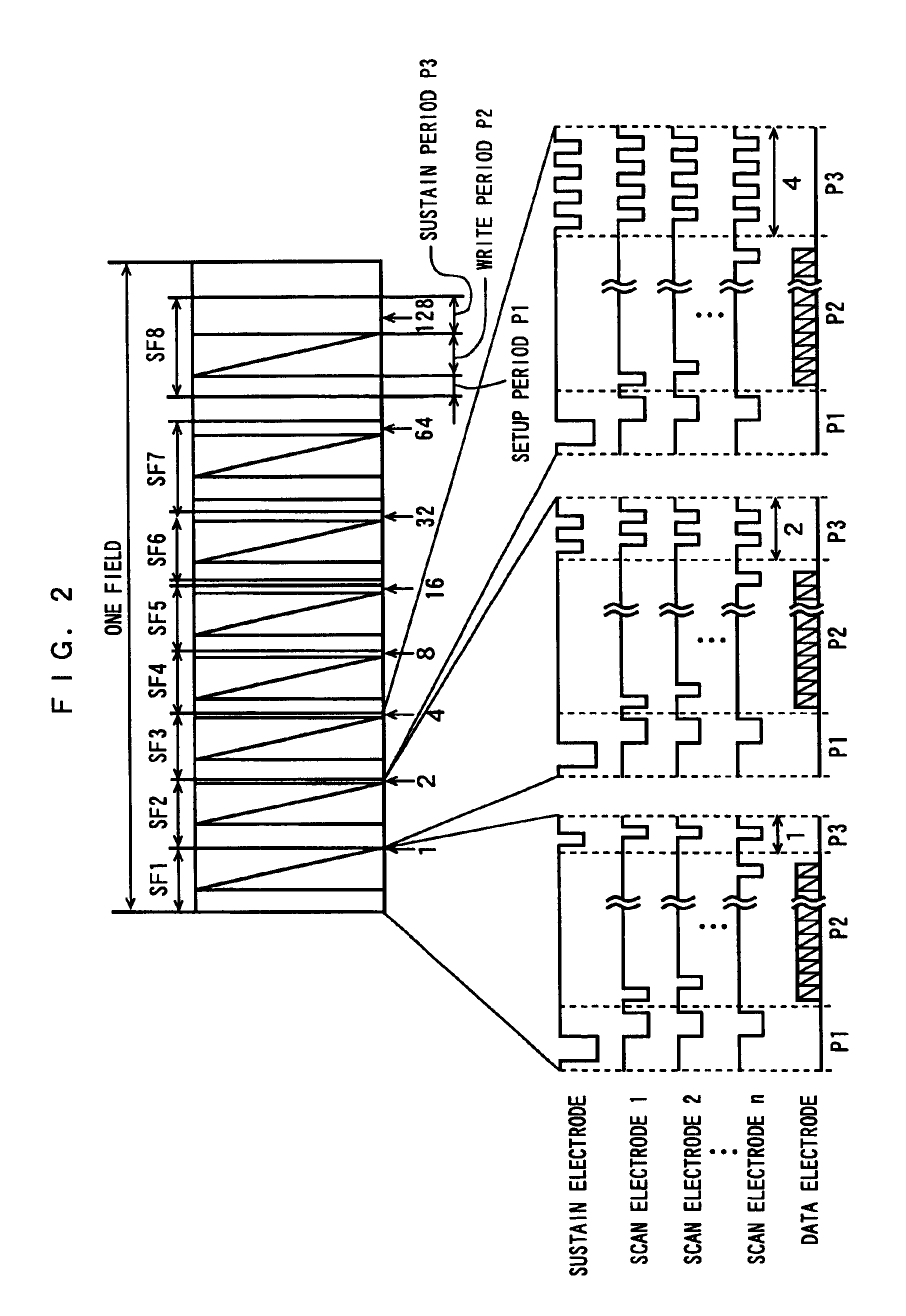
[0167]A video signal VD is inputted to the A / D converter 1. The A / D converter 1 converts the analog video signal VD into digital image data, and outputs the digital image data to the video signal / sub-field corresponder 2. The video signal / sub-field corresponder 2 divides one field into a plurality of sub-fields and displays the sub-fields. Therefore, image data SP for each of the sub-fields is generated from the image data in the one field, and is outputted to the sub-field processor...

second embodiment

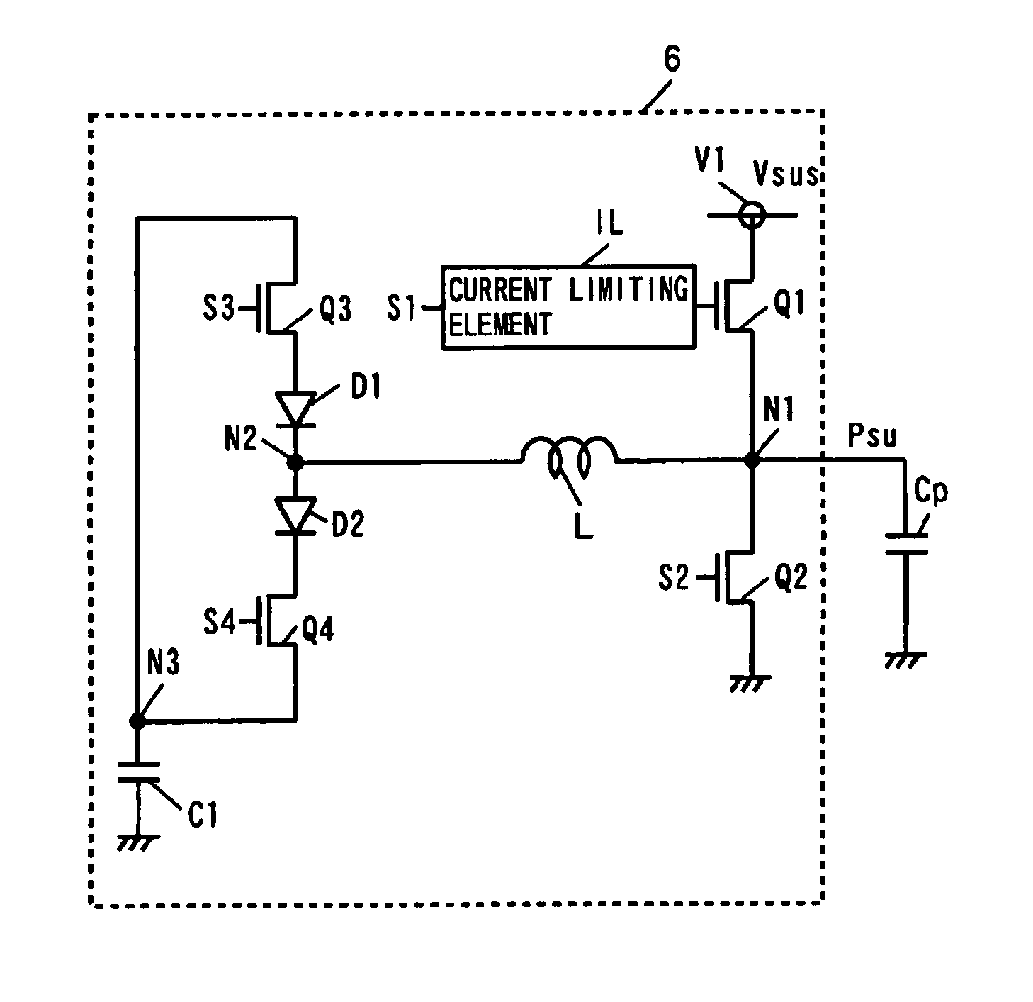
[0279]The present embodiment is the same as the second embodiment except that the scan driver 5a and the sustain driver 6a correspond to a driving circuit, first to third driving circuits and a final driving circuit, the sub-field processor 3a corresponds to a control circuit, the capacitor C2 corresponds to a second capacitive element, the variable voltage source VR corresponds to a voltage source and a variable voltage source, the voltage control circuit 9 corresponds to a voltage control circuit, the capacitor C2, the coil L1, the transistors Q5 and Q6, the diode D3, and the variable voltage source VR correspond to a second driving circuit, and a transistor Q1, a current-limiting element IL and a power supply terminal V1 correspond to a third driving circuit.

[0280]FIG. 23 is a timing chart showing the operation in a sustain time period of the sustain driver 6a shown in FIG. 22. FIG. 23 illustrates a voltage at the node N1 shown in FIG. 22, discharge intensity LR in a PDP 7, and c...

third embodiment

[0310]The voltage control circuit 9a respectively outputs a voltage control signal VC for controlling an output voltage of a variable voltage source in a scan driver 5a and a voltage control signal VU for controlling an output voltage of a variable voltage source VR in a sustain driver 6a to the scan driver 5a and the sustain driver 6a in response to the minimal value signals MC and MU. The subsequent operations of the scan driver 5a and the sustain driver 6a and an operation for controlling the waveform of the sustain pulse depending on a lighting rate for each sub-field are the same as those in the third embodiment and hence, the detailed description thereof is omitted.

[0311]The present embodiment is the same as the third embodiment except that the voltage control circuit 9a corresponds to a voltage control circuit, and the minimal value detectors 10a and 10b correspond to a potential detection circuit.

[0312]An operation for controlling a voltage of a sustain pulse depending on a ...


PUM


Abstract

A plasma display having a discharge cell, the emission efficiency of which is improved by generating first and second discharges with one sustaining pulse. A first discharge is generated by increasing a voltage up to a maximal value through a LC resonance formed by a recovery coil and a panel capacitor. A second discharge is generated by connecting the panel capacitor to a power supply when the voltage falls a predetermined amount below the maximal value, thereby increasing the voltage to a predetermined level above the maximal value.

Description

TECHNICAL FIELD[0001]The present invention relates to a display device for selectively discharging a plurality of discharge cells to display an image and a method of driving the same.BACKGROUND ART[0002]Plasma display devices using PDPs (Plasma Display Panels) have the advantage that thinning and larger screens are possible. In the plasma display devices, images are displayed by utilizing light emission in cases where discharge cells composing pixels are discharged.[0003]FIG. 46 is a diagram for explaining a method of driving discharge cells in an AC-type PDP. As shown in FIG. 46, the surfaces of electrodes 301 and 302 opposite to each other are respectively covered with dielectric layers 303 and 304 in the discharge cell in the AC-type PDP.[0004]As shown in FIG. 46(a), when a voltage lower than a discharge start voltage is applied between the electrodes 301 and 302, no discharges are induced. As shown in FIG. 46(b), when a voltage in a pulse shape (a write pulse) higher than the di...

Claims


Application Information

Patent Timeline
Patent Type & Authority Patents(United States)
IPC IPC(8): G09G3/28G09G3/294G09G3/296
CPCG09G3/294G09G3/2942G09G3/2965G09G2310/066G09G2360/16G09G2330/021G09G2330/025G09G2330/06G09G2320/0626G09G3/296
Inventor MORI, MITSUHIROKASAHARA, MITSUHIROOE, YOSHINAOTACHIBANA, HIROYUKI
Owner PANASONIC CORP
Why Eureka
Try Eureka