Liquid crystal display device and manufacturing method thereof
- Summary
- Abstract
- Description
- Claims
- Application Information
AI Technical Summary
Benefits of technology
Problems solved by technology
Method used
Image

Examples
first embodiment
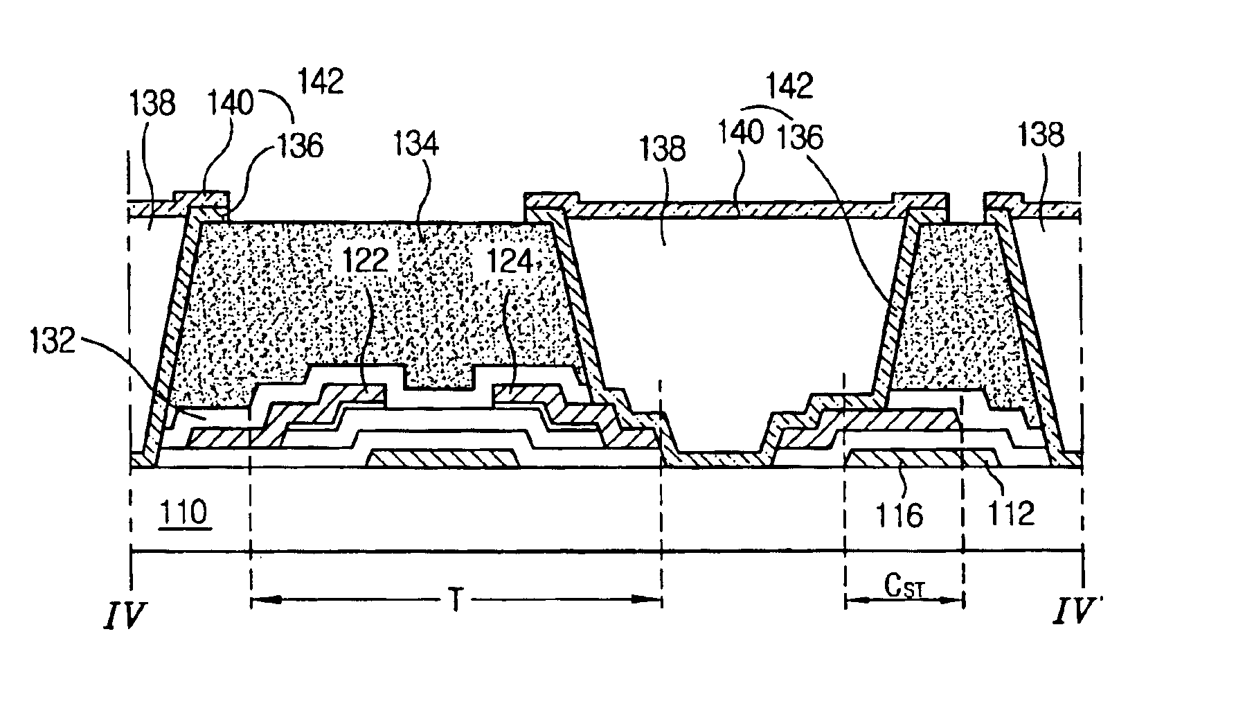
[0040]FIGS. 4A to 4I, FIGS. 5A to 5I, and FIGS. 6A to 6I are cross-sectional views illustrating process steps of manufacturing an array substrate according to the presenting invention.FIGS. 4A to 4I correspond to cross-sections along the line IV-IV′ of FIG. 3, FIGS. 5A to 5I correspond to cross-sections along the line V-V′ of FIG. 3, and FIGS. 6A to 6I correspond to cross-sections along the line VI-VI′ of FIG. 3.
[0041]Referring to FIGS. 4A, 5A and 6A, a gate electrode 114, a gate line 112 and a gate pad 117 are formed on a substrate 110 by depositing a first metal material and then patterning it through a first mask process, which is a photolithography process including the steps of light-exposing and developing photosensitive material. A part of the gate line 112 functions as a first capacitor electrode 116. The gate electrode 114 extends from the gate line 112 while the gate pad 117 is situated at one end of the gate line 112.
[0042]Referring to FIGS. 4B, 5B and 6B, a gate insulati...
second embodiment
[0051]FIGS. 7A to 7F, FIGS. 8A to 8F and FIGS. 9A to 9F are cross-sectional views illustrating process steps of manufacturing an array substrate according to the presenting invention, and uses some of the same steps as discussed in reference to FIGS. 4A to 4D, FIGS. 5A to 5D and FIGS. 6A to 6D. Thus, explanation for the steps that are also used in FIGS. 4A to 4D, FIGS. 5A to 5D and FIGS. 6A to 6D will be omitted, and the number of mask processes will also not be mentioned. Wherever possible, the same reference numbers will be used throughout the drawings to refer to the same or like parts.
[0052]Referring to FIGS. 7A, 8A and 9A, after the passivation layer 232 is formed in the steps described with regard to FIGS. 4A to 4D, FIGS. 5A to 5D and FIGS. 6A to 6D of FIGS. 4D, 5D and 6D, a gate pad contact hole 219 exposing the gate pad 217 is formed in the passivation layer 232 and gate insulating layer 218 by removing the passivation layer 232 and gate insulating layer 218 over the gate pa...
third embodiment
[0059]FIGS. 10A to 10E, FIGS. 11A to 11E and FIGS. 12A to 12E are cross-sectional views illustrating process steps of manufacturing an array substrate according to the presenting invention, and follow the steps discussed in reference to FIGS. 4A to 4D, FIGS. 5A to 5D and FIGS. 6A to 6D. Thus, explanation for the steps of FIGS. 4A to 4D, FIGS. 5A to 5D and FIGS. 6A to 6D will be omitted, and the number of mask processes will also not be mentioned. Wherever possible, the same reference numbers will be used throughout the drawings to refer to the same or like parts.
[0060]Referring to FIGS. 10A, 11A and 12A, after a first passivation layer 332, which is referred to as a passivation layer 132 in FIGS. 4D, 5D and 6D, is formed in the step of FIGS. 4D, 5D and 6D, a black matrix 334 is formed on the first passivation layer 332 by forming a light-blocking material and patterning it. Next, a second passivation layer 335 is formed on an entire surface of the substrate 310 including the black m...
PUM
 Abstract
Description
Claims
Application Information
 - Generate Ideas
- Intellectual Property
- Life Sciences
- Materials
- Tech Scout
- Unparalleled Data Quality
- Higher Quality Content
- 60% Fewer Hallucinations
Browse by: Latest US Patents, China's latest patents, Technical Efficacy Thesaurus, Application Domain, Technology Topic, Popular Technical Reports.
© 2025 PatSnap. All rights reserved.Legal|Privacy policy|Modern Slavery Act Transparency Statement|Sitemap|About US| Contact US: help@patsnap.com