Pattern transfer method using a mask and half tone mask

a technology of mask and mask, applied in the field of pattern transfer, can solve the problems of difficult minimization of resolution pattern, degrade device performance, difficulty in realizing a larger-scale integrated semiconductor pattern, etc., and achieve the effect of preventing the difference in resist siz

Inactive Publication Date: 2005-06-07
SHARP KK
View PDF9 Cites 18 Cited by
  • Summary
  • Abstract
  • Description
  • Claims
  • Application Information

AI Technical Summary

Benefits of technology

[0019]An object of the present invention is to provide a half tone mask, and a pattern transfer method using the half tone mask, which can prevent the difference in size of a resist between a dense pattern area and an isolated pattern area due to optical proximity effect which occurs in the dense pattern area.

Problems solved by technology

However, the optical proximity effect, which occurs in the dense pattern area, causes distortion of light intensity distribution curve in the exposure (transmission light through the mask), and the patterns formed on the resist in the dense pattern area becomes larger in size than the pattern in the isolated pattern area where no optical proximity effect occurs, though their opening sections are the same in size on the mask.
The conventional half tone mask can raise resolution to be higher than that in the case of a chrome mask by making the sharpest curve in light intensity distribution, but the difference in size of the resist between the dense pattern area and the isolated pattern area degrades the performance of the device, and makes minimization of resolution pattern difficult.
Thus, it causes a difficulty of realizing a larger-scale integrated semiconductor pattern.

Method used


Image

  • Pattern transfer method using a mask and half tone mask
  • Pattern transfer method using a mask and half tone mask
  • Pattern transfer method using a mask and half tone mask

Examples


embodiment 1

[Embodiment 1]

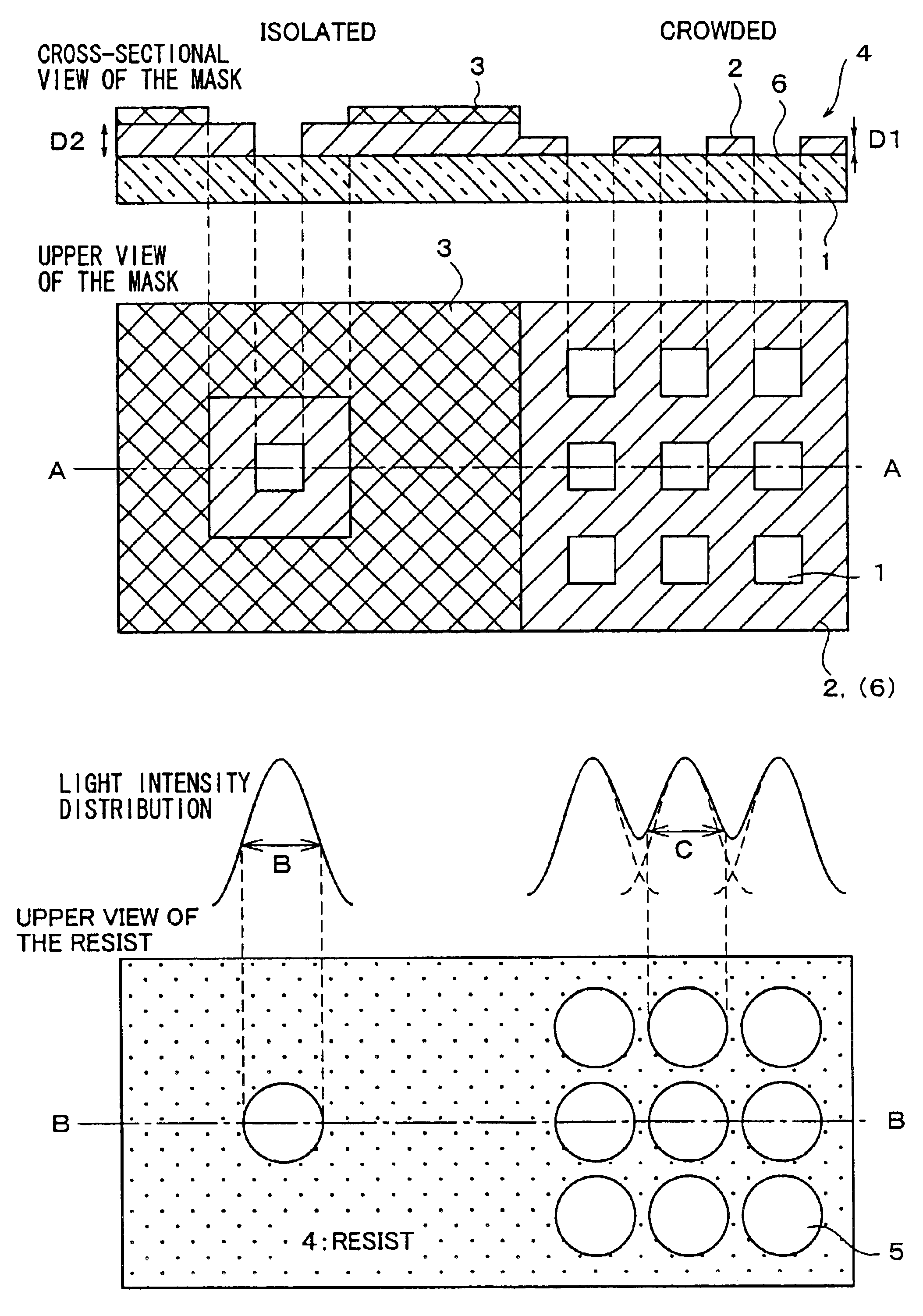
[0047]FIG. 1(a) is a cross-sectional view and an upper view of a half tone mask according to the present embodiment. FIG. 1(b) shows a state of light intensity distribution curve in the exposure, and the size of the contact hole formed on a resist, when exposure of the resist is performed by using the half tone mask of the present embodiment.

[0048]Note that, the cross-sectional view of the mask in FIG. 8(a) is taken along the line A—A in the upper view of the mask, and the light intensity distribution in FIG. 8(b) is taken at the line B—B in the upper view of the mask.

[0049]As shown in FIG. 1(a), the half tone mask of the present embodiment has a three-layers structure in which a half tone film 2 is selectively provided on a transparent substrate 1, and a light blocking film 3 is further formed on the half tone film 2.

[0050]The thickness of the half tone film 2 differs respectively in a dense pattern area (having dense patterns) and an isolated pattern area (having an ...

embodiment 2

[Embodiment 2]

[0085]FIG. 5(a) is a cross-sectional view and an upper view of a half tone mask according to another embodiment of the present invention. FIG. 5(b) shows a state of light intensity distribution curve in the exposure, and the size of the contact hole formed on a resist, when exposure of the resist is performed by using the half tone mask of the present embodiment.

[0086]Note that, the cross-sectional view of the mask in FIG. 8(a) is taken along the line A—A in the upper view of the mask, and the light intensity distribution in FIG. 8(b) is taken at the line B—B in the upper view of the mask.

[0087]Note that, for ease of explanation, materials having the equivalent functions as those shown in the drawings pertaining to Embodiment 1 above will be given the same reference symbols, and explanation thereof will be omitted here.

[0088]As shown in FIG. 5, in the half tone mask of the present embodiment, the thickness of the half tone film 2, which is selectively provided on the t...


PUM

PropertyMeasurementUnit
thicknessaaaaaaaaaa
thicknessaaaaaaaaaa
hole sizeaaaaaaaaaa

Abstract

A half tone mask of the present invention is provided with a half tone film in which a thickness of the half tone film in a dense pattern area where optical proximity effect occurs differs from that in an isolated pattern area where the optical proximity effect does not occur, the thickness of the half tone film in the isolated pattern area being adjusted so that difference in size of a resist does not occur between the dense pattern area and the isolated pattern area due to the optical proximity effect, thus preventing the difference in size of the resist between the dense pattern area and the isolated pattern area, even when providing high definition patterns which causes the optical proximity effect.

Description

FIELD OF THE INVENTION[0001]The present invention relates to a pattern transfer method using a mask for optical lithography, half tone mask and a manufacturing method of the half tone mask, and a manufacturing method of a circuit board, which are suitably adopted for a manufacturing of a circuit board of such as an LSI (Large Scale Integrated Circuit).BACKGROUND OF THE INVENTION[0002]In recent years, remarkable progress of miniaturization of semiconductor devices has been made, and its processing rule has fallen under the realm of wavelength of light for exposure. With the progress, a new problem of the difference in size of the resist has arisen. The difference in size occurs between a dense pattern area having many gathered patterns, and an isolated pattern area having only one pattern, since optical proximity effect occurs in the dense pattern area and does not occur in the isolated pattern area. This difference in size of the resist degrades performance of the semiconductor devi...

Claims


Application Information

Patent Timeline
Patent Type & Authority Patents(United States)
IPC IPC(8): G03F1/00H05K3/00G03F1/32G03F1/36G03F1/54G03F1/68G03F7/20H01L21/027
CPCG03F1/32H05K3/0002G03F1/29H01L21/027
Inventor WATANABE, KUNIO
Owner SHARP KK
Why Eureka
Try Eureka