Band pass filter

a filter and band pass technology, applied in the direction of waveguides, basic electric elements, electrical equipment, etc., can solve the problems of difficult achieving both the super sharp cut and the very narrow band, and the realization of the very narrow band super sharp cut filter is very difficul

Active Publication Date: 2005-06-07
KK TOSHIBA
View PDF2 Cites 11 Cited by
  • Summary
  • Abstract
  • Description
  • Claims
  • Application Information

AI Technical Summary

Benefits of technology

[0014]It is an object of the present invention to provide a narrow band sharp cut band pass filter by stabilizing weak coupling between resonators.

Problems solved by technology

However, in a high frequency band in particular, a super sharp cut filter is desirable in order to cut an adjacent signal in a very narrow band, but realization of such a very narrow band super sharp cut filter is very difficult.
However, achieving both the very narrow band and the super sharp cut is difficult.
As described above, realization of a very narrow band super sharp cut filter is very difficult, by using a conventional filter.
There are two problems when realizing the super sharp cut filter.
379, all the couplings become weak when each distance between the resonators is increased, but coupling of the resonators other than adjacent resonators does not become sufficiently weak.
Therefore, the characteristic is disadvantageously disrupted when the coupling is adjusted by using the distance between the resonators to obtain a very narrow bandwidth filter.
Additionally, since the distance between the resonators must be largely increased, the filter itself becomes large in size, a problem of a limitation in size of a substrate and the like restricts the design.
Also, the sufficient number of resonators cannot be assured, and hence the sharp cut cannot be realized.
Another important problem becomes apparent when configuring the very narrow band sharp cut filter with a low insertion loss.
In the regular Chebychev type filter, the number of resonators is increased in order to realize the sharp cut, but this is very disadvantageous in terms of the loss in case of the narrow band, and the insertion loss is greatly increased.
This considerably disrupts the characteristic, and there occurs a problem that the sharp cut pseudo-elliptic function type filter cannot be successfully realized in the narrow band.
In this filter, however, spatial coupling between the resonators is also used for coupling between the adjacent resonators, but all the designed weak couplings are hard to be taken, thereby making it difficult to realize the very narrow band filter successfully.
Additionally, in regard to non-adjacent coupling based on this transmission line path, there is a serious problem.
This is a problem that an original resonance frequency of the resonators deviates by adding a transmission line path for coupling.
In the very narrow band filter, since the band is originally very narrow, the filter is very sensitive to spatial distribution or the like of material parameters, adding such a deviation of the resonance frequency to this property results in a serious problem.
For example, in the case of coupling the resonators, when a center frequency of each resonator is out of this band, which is assumed to be very narrow, realization of the band pass filter becomes very difficult.
As described above, the very narrow band sharp cut filter using a planar structure circuit is hard to realize based on only the prior art.

Method used


Image

  • Band pass filter
  • Band pass filter
  • Band pass filter

Examples


embodiment 1

[0056]FIG. 10 is a plane view for illustrating one pattern of a filter according to an embodiment 1 of the present invention.

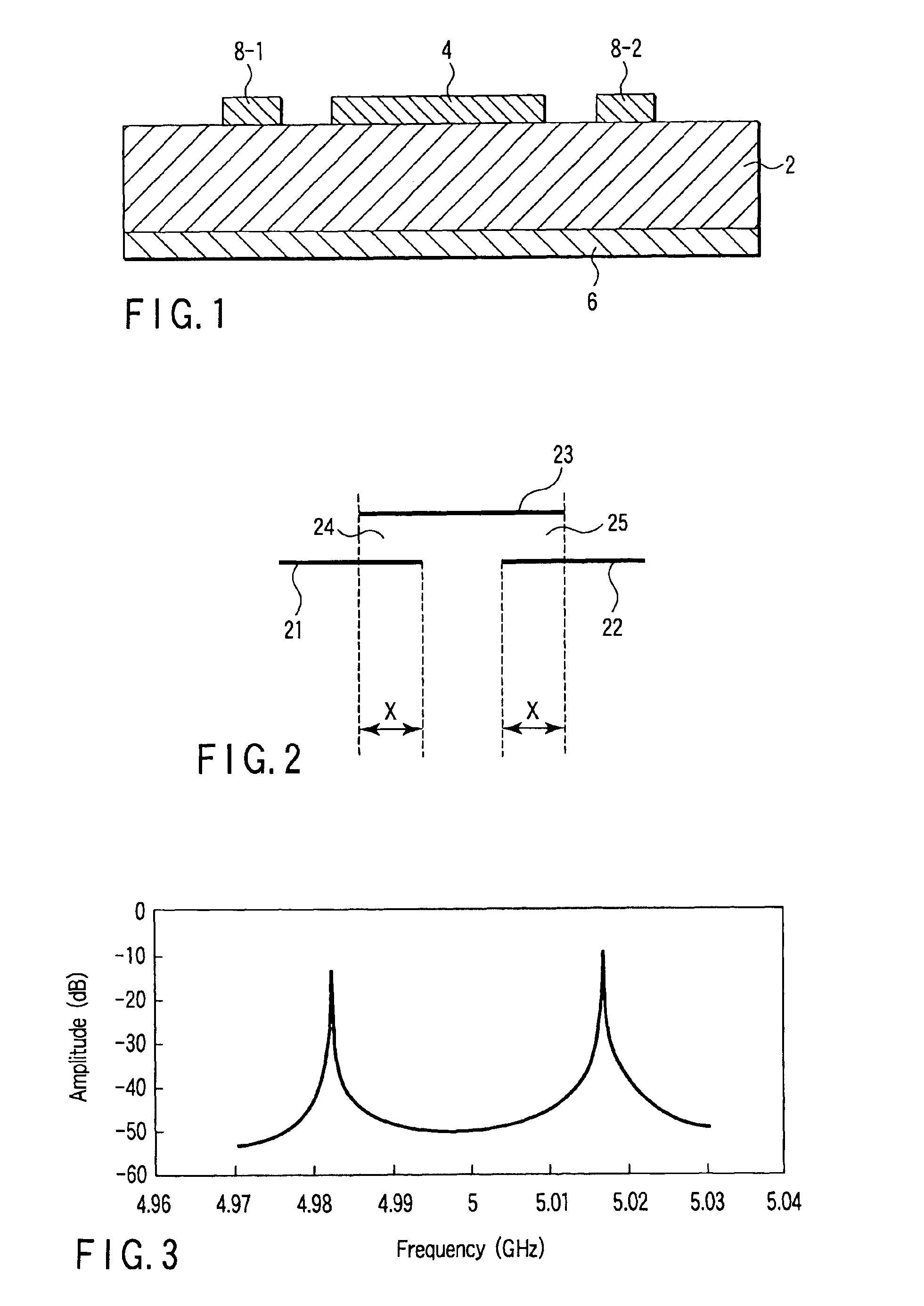
[0057]Like the description based on FIG. 1, a superconducting microstrip line is formed on an MgO substrate 2 having a thickness of approximately 0.43 mm and a relative dielectric constant of approximately 10. Here, a Y-based copper oxide high-temperature superconducting thin film having a thickness of approximately 500 nm is used as a superconductor of the microstrip line, and a line width of a strip conductor is approximately 0.4 mm. The superconducting thin film 4 is manufactured by a laser evaporation method, a sputtering method, a codeposition method or the like.

[0058]The filter shown in FIG. 10 is a Chebychev type filter including six resonators 32, 34, 36, 38, 40 and 42 between input / output line paths 31 and 43 formed by excitation lines. The six half-wavelength hairpin type resonators 32, 34, 36, 38, 40 and 42 whose open sides are directed in the same ...

embodiment 2

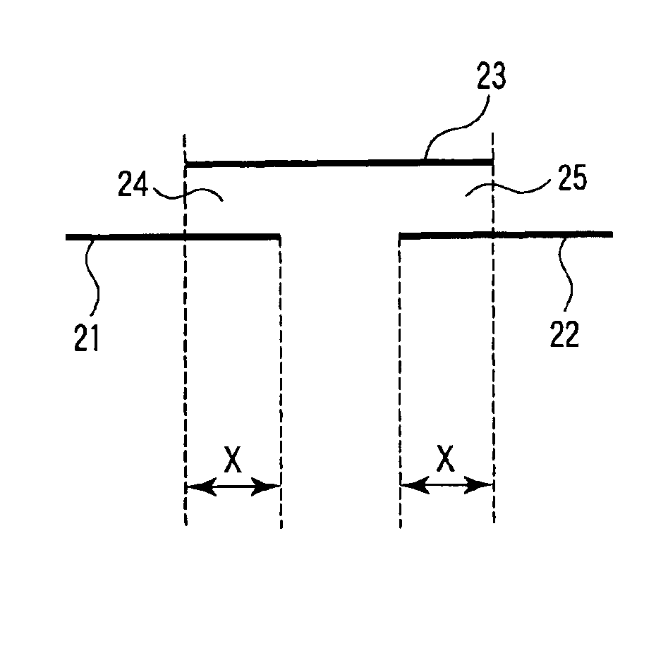
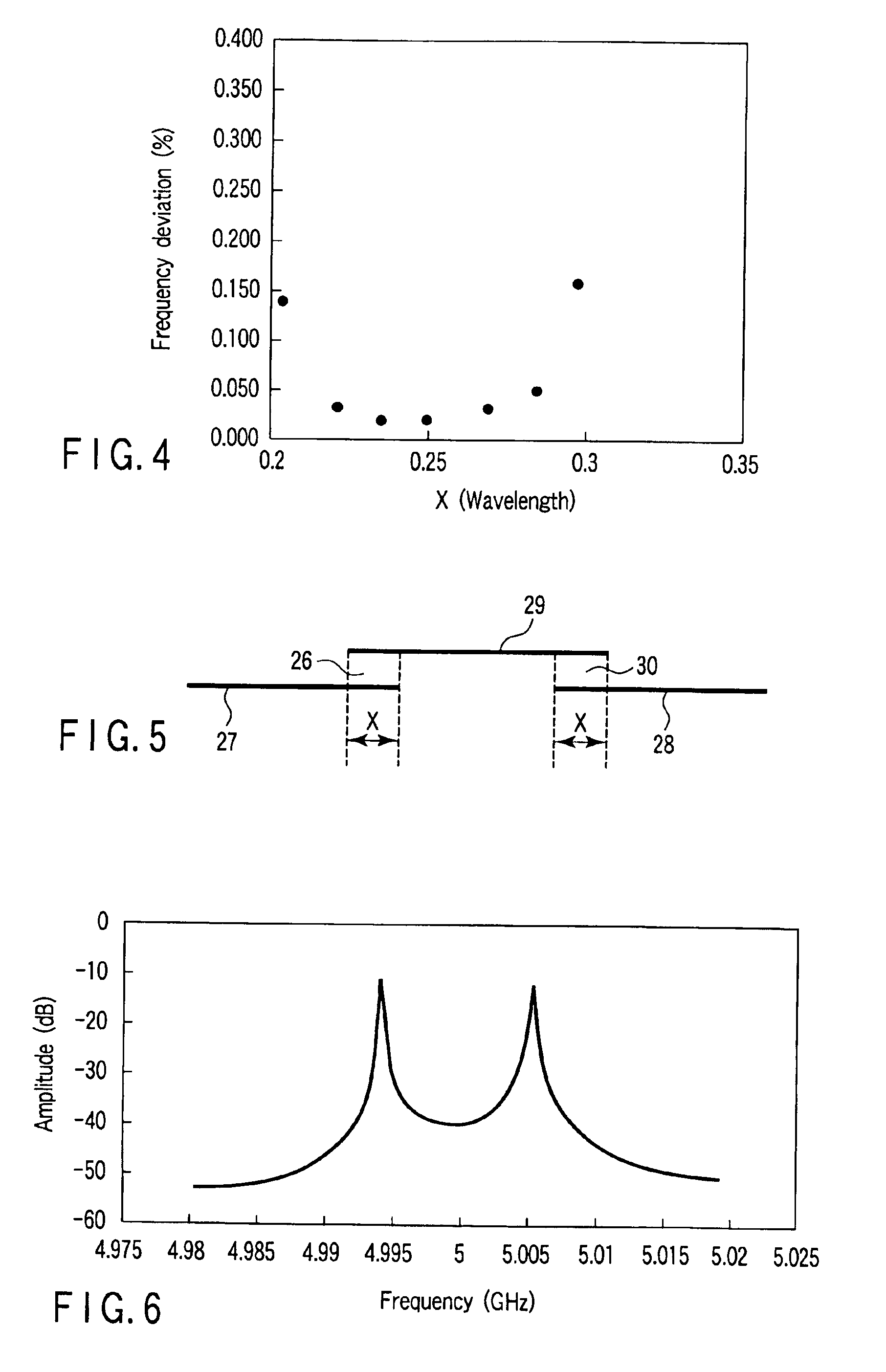
[0060]FIG. 12 is a plane view for illustrating one pattern of a filter according to another embodiment of the present invention. The filter shown in FIG. 12 is a Chebychev filter including four resonators 51, 53, 55 and 57 between input / output line paths 50 and 58 formed by excitation lines. As the resonators, there are used one-wavelength linear type resonators 51, 53, 55 and 57. Therefore, a wavelength corresponding to a resonance frequency matches a length of each resonator. Additionally, the resonators 51, 53, 55 and 57 adjacent to each other are coupled through line paths 52, 54 and 56 bent into such a shape as shown in FIG. 8, respectively. Each of the transmission line paths 52, 54 and 56 has a length of a {fraction (7 / 4)} wavelength, a length x of each coupling portion is substantially determined as a ¼ wavelength, and this coupling portion is arranged in closest proximity to a corresponding resonator. As described above, since the length of each resonator is determined as o...

embodiment 3

[0063]FIG. 14 is a plane view for illustrating one pattern of a filter according to still another embodiment of the present invention.

[0064]In the filter shown in FIG. 14, a superconducting microstrip line path is formed on an MgO substrate (not shown) having a thickness of approximately 0.43 mm and a relative dielectric constant of 10. Here, a Y-based copper oxide high-temperature superconducting thin film having a thickness of approximately 500 nm is used as a superconductor of the microstrip line, and a line width of a strip conductor is approximately 0.4 mm. The superconducting thin film is manufactured by a laser evaporation method, a sputtering method, a codeposition method or the like.

[0065]The filter shown in FIG. 14 is a four-stage filter constituted by four linear resonators 61, 63, 65 and 67 provided between input / output line paths 60 and 68 formed by excitation lines. In the filter depicted in FIG. 14, a one-wavelength resonator is used as each resonator, and the adjacen...


PUM

PropertyMeasurementUnit
lengthaaaaaaaaaa
thicknessaaaaaaaaaa
thicknessaaaaaaaaaa

Abstract

A band pass filter configured by a planar structure circuit, includes resonators of distribution constant circuit type, transmission line paths coupling the resonators and excitation lines arranged at input/output sides. The transmission line path is provided with line path portions coupling the resonators or the resonator and the excitation line. The line path portion have a length which is (1+2m)/4-fold (m: natural number) of a wavelength corresponding to a center frequency of the frequency band, and each coupling part between the resonators and the line portion has a length substantially determined as a ¼ wavelength.

Description

CROSS-REFERENCE TO RELATED APPLICATIONS[0001]This application is based upon and claims the benefit of priority from the prior Japanese Patent Application No. 2003-142239, filed May 20, 2003, the entire contents of which are incorporated herein by reference.BACKGROUND OF THE INVENTION[0002]1. Field of the Invention[0003]The present invention relates to a band pass filter, and more particularly to a band pass filter for use in communication devices.[0004]2. Description of the Related Art[0005]A band pass filter is a component which is needed to prevent interference of signals and effectively utilize a frequency. In the field of communications, performance of a filter is particularly important, as it determines an effective use of a frequency which is an important resource. That is, in regard to an electromagnetic wave transmitted / received by an antenna, an out-of-band signal is cut by a reception filter or a transmission filter, thereby greatly reducing interferences with an adjacent ...

Claims


Application Information

Patent Timeline
Patent Type & Authority Patents(United States)
IPC IPC(8): H01P1/203H01P1/20H01P1/205
CPCH01P1/20381
Inventor HASHIMOTO, TATSUNORIAIGA, FUMIHIKOFUKE, HIROYUKITERASHIMA, YOSHIAKIYAMAZAKI, MUTSUKIKAYANO, HIROYUKI
Owner KK TOSHIBA
Why Eureka
Try Eureka