Solution processed devices

a technology of processing device and dielectric layer, applied in the direction of solid-state device, transistor, material nanotechnology, etc., can solve the problems of difficult fabrication of via-hole through dielectric layer, severe limitations on the choice of semi-conducting materials, and the use of semi-conducting materials

Inactive Publication Date: 2005-06-14
FLEHKSENEHBL LTD
View PDF21 Cites 71 Cited by
  • Summary
  • Abstract
  • Description
  • Claims
  • Application Information

AI Technical Summary

Benefits of technology

[0089]FIGS. 15(a), 15(b), 15(c) and 15(d) show applications of via holes such as logic inverters (d...

Problems solved by technology

However, it severely limits the choice of semiconducting materials, that can be used, to the small and in several respects undesirable class of precursor polymers.
Furthermore, cross-linki...

Method used


Image

  • Solution processed devices
  • Solution processed devices
  • Solution processed devices

Examples


Embodiment Construction

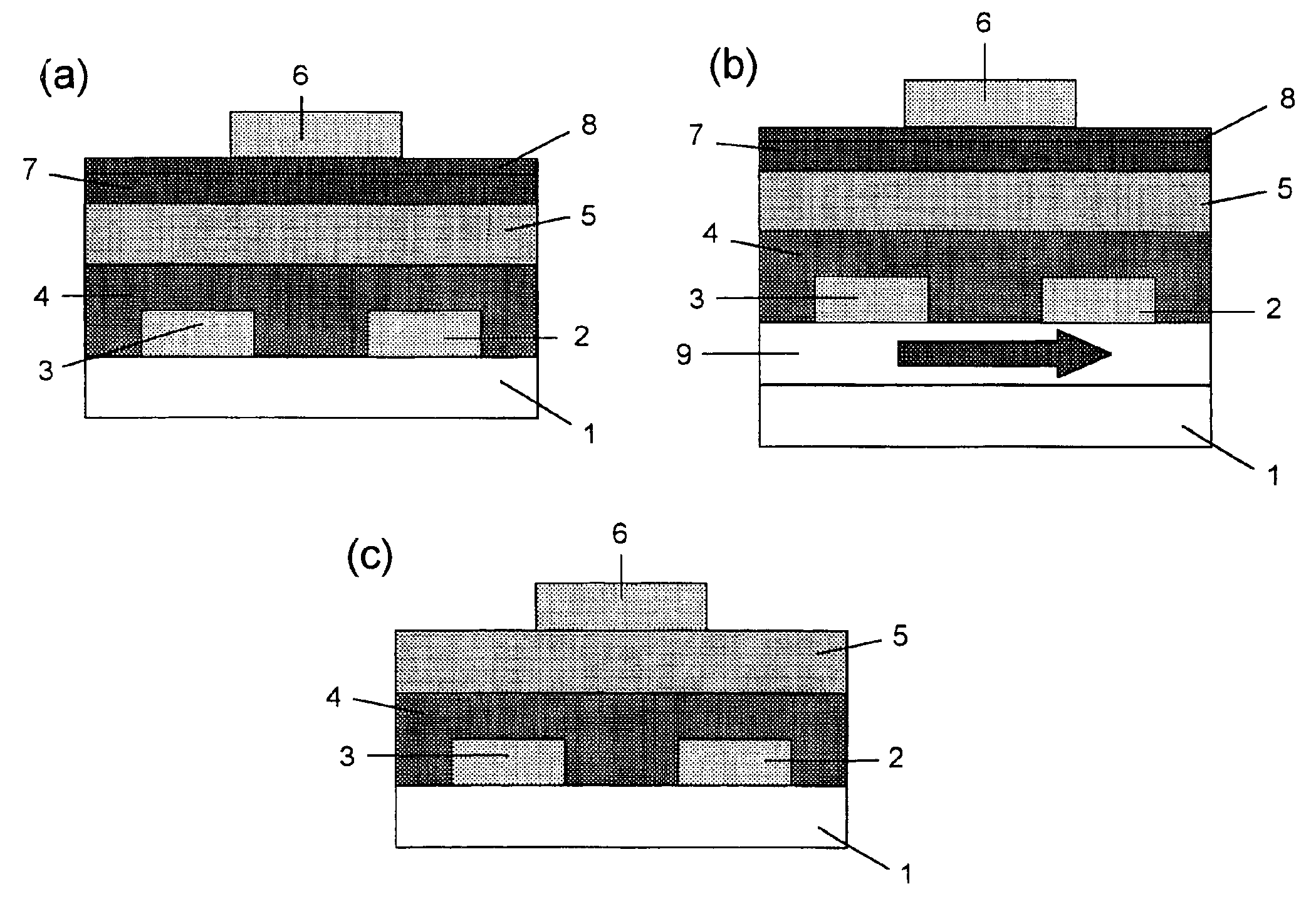
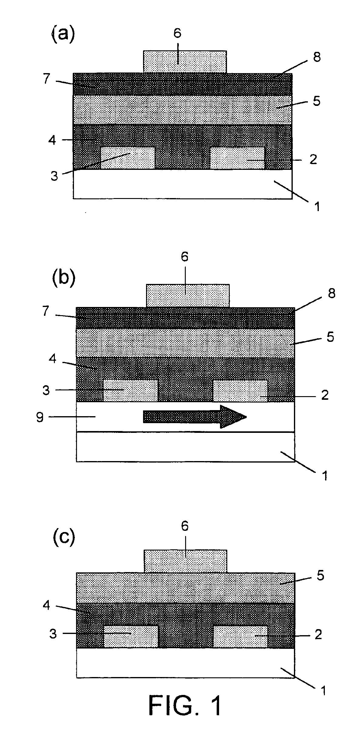
[0097]Preferred fabrication methods described herein permit the fabrication of an all-organic, solution-processed thin-film transistor, in which none of the layers is converted or cross-linked into an insoluble form. Each layer of such a device may remain in a form that is soluble in the solvent from which it was deposited. As will be described in more detail below, this enables a simple way of fabricating via-holes through dielectric insulating layers based on local deposition of solvents. Such a device may, for example, comprise one or more of the following components:[0098]patterned conducting source-drain and gate electrodes and interconnects.[0099]a semiconducting layer with a charge carrier mobility exceeding 0.01 cm2 / Vs and a high ON-OFF current switching ratio exceeding 104.[0100]a thin gate insulating layer.[0101]a diffusion barrier layer that protects the semiconducting layer and the insulating layer against unintentional doping by impurities and ionic diffusion.[0102]a su...


PUM


Abstract

A method for forming a transistor, comprising: depositing a first material from solution in a first solvent to form a first layer of the transistor, and subsequently whilst the first material remains soluble in the first solvent, forming a second layer of the transistor by depositing over the first material a second material from solution in a second solvent in which the first material is substantially insoluble.

Description

[0001]This is a Continuation-In-Part of Application No. PCT / GB00 / 04934 filed Dec. 21, 2000; the disclosure of which is incorporated herein by reference.[0002]This invention relates to solution processed devices and methods for forming such devices.BACKGROUND OF THE INVENTION[0003]Semiconducting conjugated polymer thin-film transistors (TFTs) have recently become of interest for applications in cheap, logic circuits integrated on plastic substrates (C. Drury, et al., APL 73, 108 (1998)) and optoelectronic integrated devices and pixel transistor switches in high-resolution active-matrix displays (H. Sirringhaus, et al., Science 280, 1741 (1998), A. Dodabalapur, et al. Appl. Phys. Lett. 73, 142 (1998)). In test device configurations with a polymer semiconductor and inorganic metal electrodes and gate dielectric layers high-performance TFTs have been demonstrated. Charge carrier mobilities up to 0.1 cm2 / Vs and ON-OFF current ratios of 106-108 have been reached, which is comparable to th...

Claims


Application Information

Patent Timeline
IPC IPC(8): H01L21/02H01L21/70H01L21/768H01L21/311H01L51/40H01L51/05H01L27/32H01L27/28H01L21/28H01L21/336H01L29/786H01L51/00H01L51/30
CPCB82Y30/00H01L21/31133H01L21/76838H01L51/0004H01L51/0545H01L51/0021H01L51/052H01L51/0541H01L51/0012H01L27/283H01L27/32H01L51/0018H01L51/002H10K19/10H10K59/00H10K71/13H10K71/191H10K71/233H10K71/30H10K71/60H10K10/471H10K10/464H10K10/466
Inventor SIRRINGHAUS, HENNINGKAWASE, TAKEOFRIEND, RICHARD HENRY
Owner FLEHKSENEHBL LTD
Why Eureka
Try Eureka