Field programmable gate array assembly

a gate array and field technology, applied in the field of integrated circuits, can solve the problems of customization, high speed, and high complexity of circuit technology used for fpga, and achieve the effect of flexible programmability with functionality and/or electrical performance characteristics

Inactive Publication Date: 2005-06-14
ALCATEL-LUCENT USA INC
View PDF10 Cites 61 Cited by
  • Summary
  • Abstract
  • Description
  • Claims
  • Application Information

AI Technical Summary

Benefits of technology

[0004]The need is met and an advance in the art is accomplished by a new class of integrated circuit assemblies in accordance with the present invention. In particular a programmable integrated circuit (IC) is combined with an integrated circuit or other device to offer the flexibility of programmability with functionality and / or electrical performance characteristics typically unavailable in a programmable IC.

Problems solved by technology

Even though FPGAs are highly flexible (e.g., programmable I / O) and under certain circumstances exhibit lower unit costs, they nevertheless fall short of the primary benefits offered by ASIC's, namely, customization, diverse function complexity and high speed.
Also, a circuit technology used for an FPGA may not be suitable to implement a certain feature, for example, a feature requiring a semiconductor technology that is different from the technology used to implement the FPGA.

Method used


Image

  • Field programmable gate array assembly
  • Field programmable gate array assembly
  • Field programmable gate array assembly

Examples


Embodiment Construction

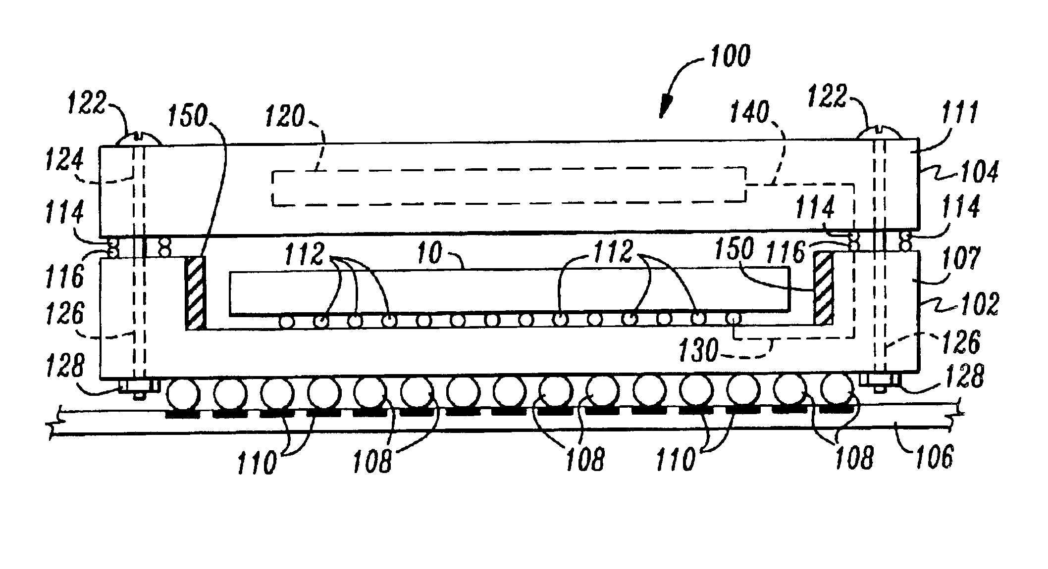
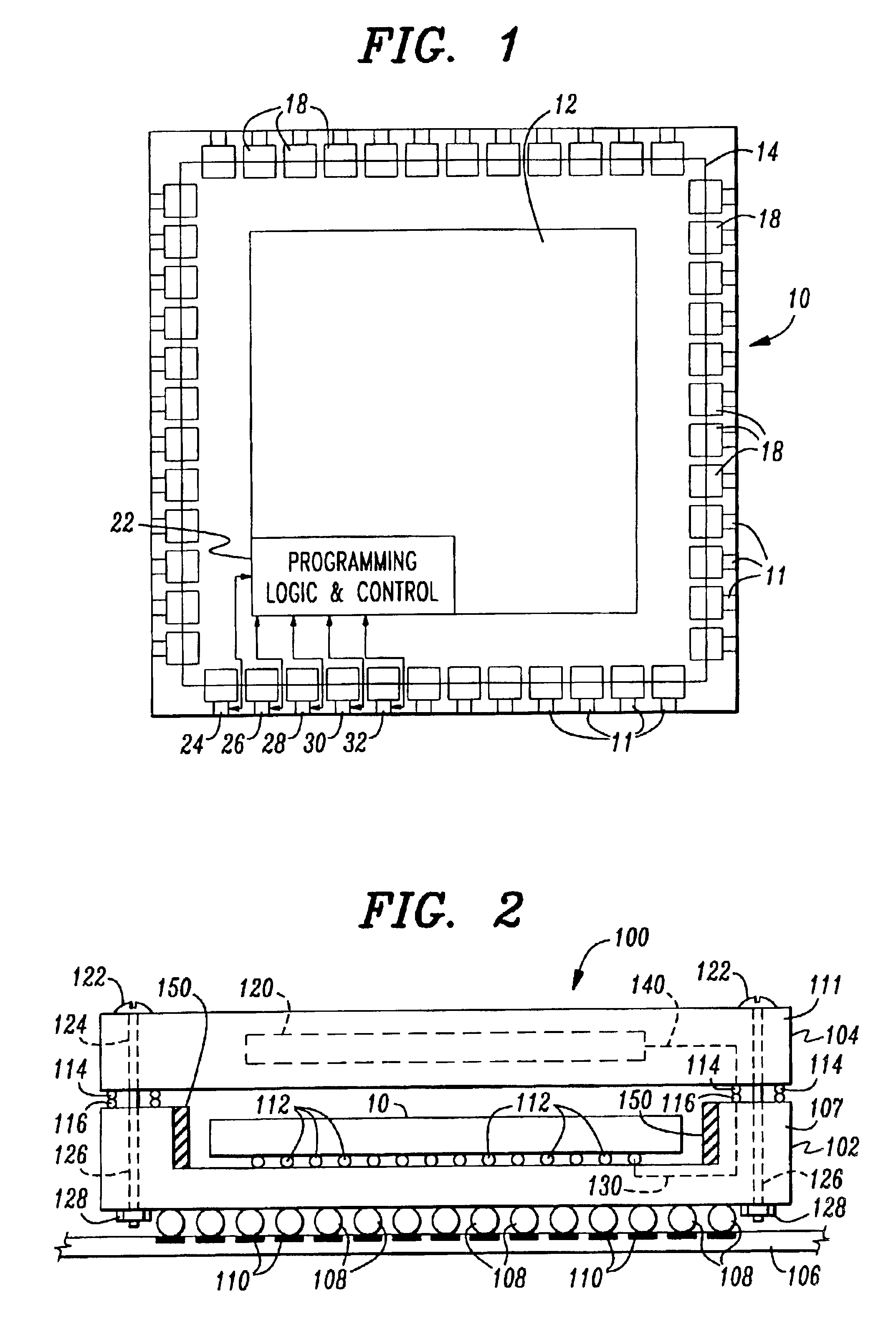
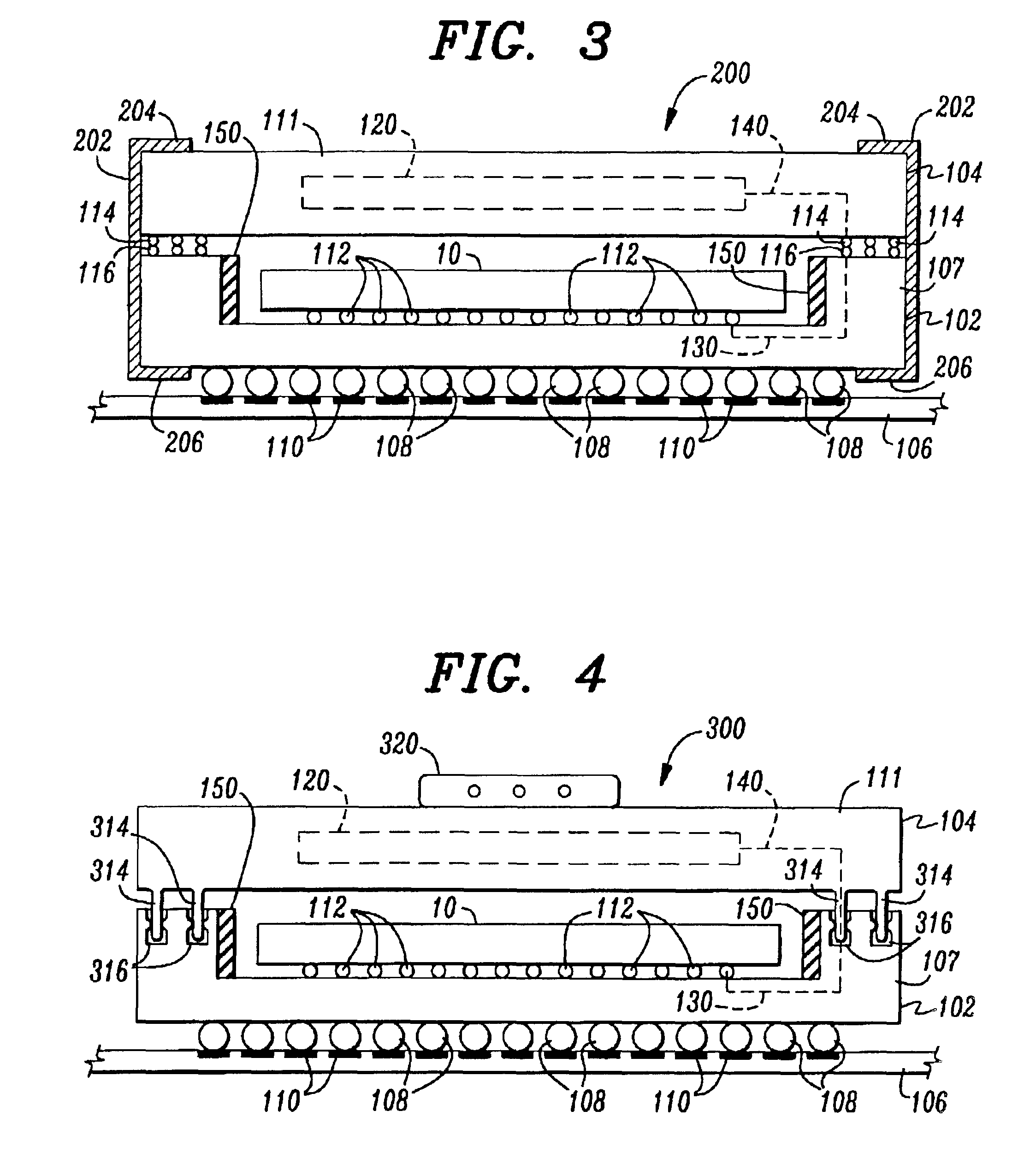
[0011]FIG. 1 is a schematic top view of a programmable integrated circuit (IC) die 10, such as, for example, a die for a field programmable gate array (FPGA). A functional core 12 is shown in the center of die 10. Bonding pads 11, which are also called I / O pads, are provided along a perimeter of die 10. Each bonding pad is coupled to a programmable I / O cell 18. Programmable I / O cells 18 provide the interface for programming the function and characteristics for the inputs and outputs of die 10. Functional core 12 includes a predetermined number of digital logic gates and cells for configuring the logic gates. Functional core 12 also includes a programming logic and control section 22 that is used to configure the internal cells, logic gates and I / O cells. Routing layers 14 provide signal paths (not shown) between programmable I / O cells 18 and functional core 12. Programming control is accomplished through pads 24, 26, 28, 30 and 32. Programmable gate arrays (PGAs) and other programma...


PUM


Abstract

A field programmable gate array assembly (100, 200, 300) offers the unique functionality typically reserved for custom ICs and application specific integrated circuits (ASICs) with the flexibility of a programmable gate array. This is accomplished by modifying a package for a programmable IC (102), such as a programmable gate array, to electrically and mechanically couple to another IC (104). The preferred electrical and mechanical coupling occurs by stacking the IC on the programmable IC.

Description

FIELD OF THE INVENTION[0001]The present invention relates to the field of integrated circuits (ICs) and in particular to the field of application specific integrated circuits (ASICs) and field programmable gate arrays (FPGAs).BACKGROUND OF THE INVENTION[0002]Application specific integrated circuits (ASICs) offer the electronics designer the ability to customize standard integrated circuits (ICs) to provide a unique set of performance characteristics by integrating complex functionality and input / output (I / O) on a single integrated circuit (IC). The significant benefits regarding the use of ASICs are customization, the ability to create unique functionality, and economies of scale for devices destined to be mass-produced. Alternative devices, such as, for example, field programmable gate arrays (FPGAs) permit the digital logic designer access to standard digital logic functions and capabilities, and additionally allow certain functions and I / O to be programmed rather than fixed durin...

Claims


Application Information

Patent Timeline
Patent Type & Authority Patents(United States)
IPC IPC(8): H01L25/065H01L25/10H01L25/16H05K3/22H05K1/18
CPCH01L25/0657H01L25/16H05K3/222H01L25/105H01L2225/1058H01L2224/16225H01L2225/06517H01L2225/0652H01L2225/06527H01L2225/06551H01L2225/06572H01L2225/06582H01L2924/15153H01L2924/15165H01L2924/15192H01L2924/15311H05K1/181H05K2201/10515H05K2201/10689H05K2201/10734H01L2924/3511
Inventor BYERS, CHARLES CALVINCOYLE, RICHARD J.
Owner ALCATEL-LUCENT USA INC
Why Eureka
Try Eureka