Multilayer substrate module and portable wireless terminal

Inactive Publication Date: 2005-06-14
MITSUBISHI ELECTRIC CORP
View PDF18 Cites 11 Cited by
  • Summary
  • Abstract
  • Description
  • Claims
  • Application Information

AI Technical Summary

Benefits of technology

[0048]In such a wireless terminal device, an orthogonal mixer is mounted on a multi-layer substrate module that is advantageous

Problems solved by technology

However, if the internal circuits provided in the multi-layer substrate module are circuits utilizing a high frequency, their operation stability may be degraded due to parasitic inductance of the ground line group.
In particular, such a problem greatly affects an internal circuit provided in the upper layer portion of the multi-layer substrate module that is subjected to increased parasitic inductance of the main ground line 150.
An integrated circuit mounted on a

Method used


Image

  • Multilayer substrate module and portable wireless terminal
  • Multilayer substrate module and portable wireless terminal
  • Multilayer substrate module and portable wireless terminal

Examples


first embodiment

[0076](First Embodiment)

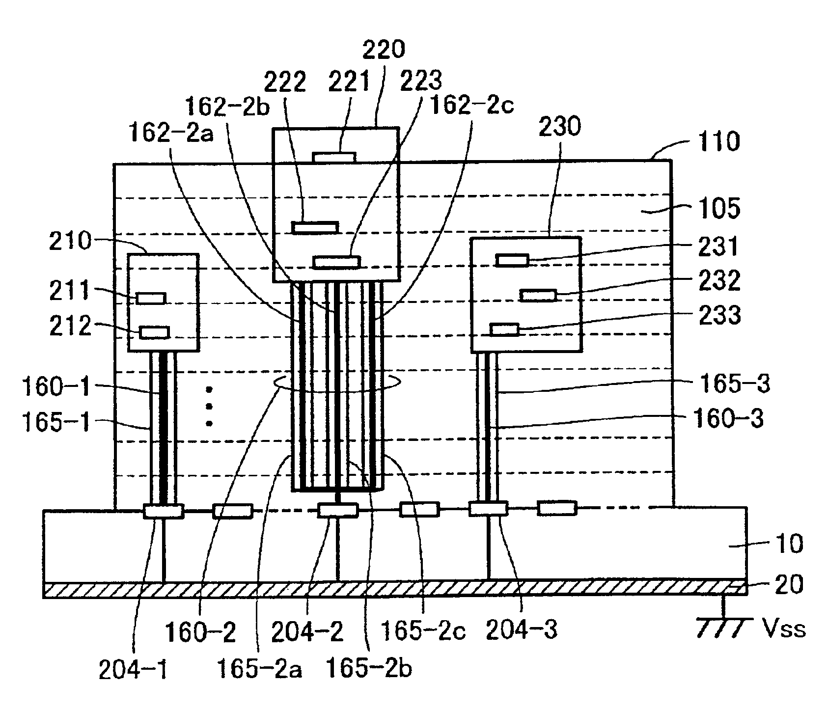
[0077]Referring to FIG. 1, a multi-layer module 110 according to the first embodiment of the present invention is mounted on a main board 10. Although not specifically shown in the figure, a plurality of wiring patterns are formed on the main board 10, and electrically coupling the wiring patterns to signal transmission nodes 202 provided as, e.g., pin terminals allows for transmission of electric signals between the main board 10 and the internal circuits formed within the multi-layer substrate module 110.

[0078]Referring to FIG. 2, the multi-layer substrate module 110 receives supply of a reference voltage Vss by connecting to an earth node 20 provided on the main board 10. Hereinafter, such supply of the reference potential Vss is sometimes simply referred to as “grounding”. For example, the wiring pattern of the earth node 20 is formed on the back surface of the main board 10, and used also for grounding the multi-layer substrate module 110.

[0079]At least ...

second embodiment

[0088](Second Embodiment)

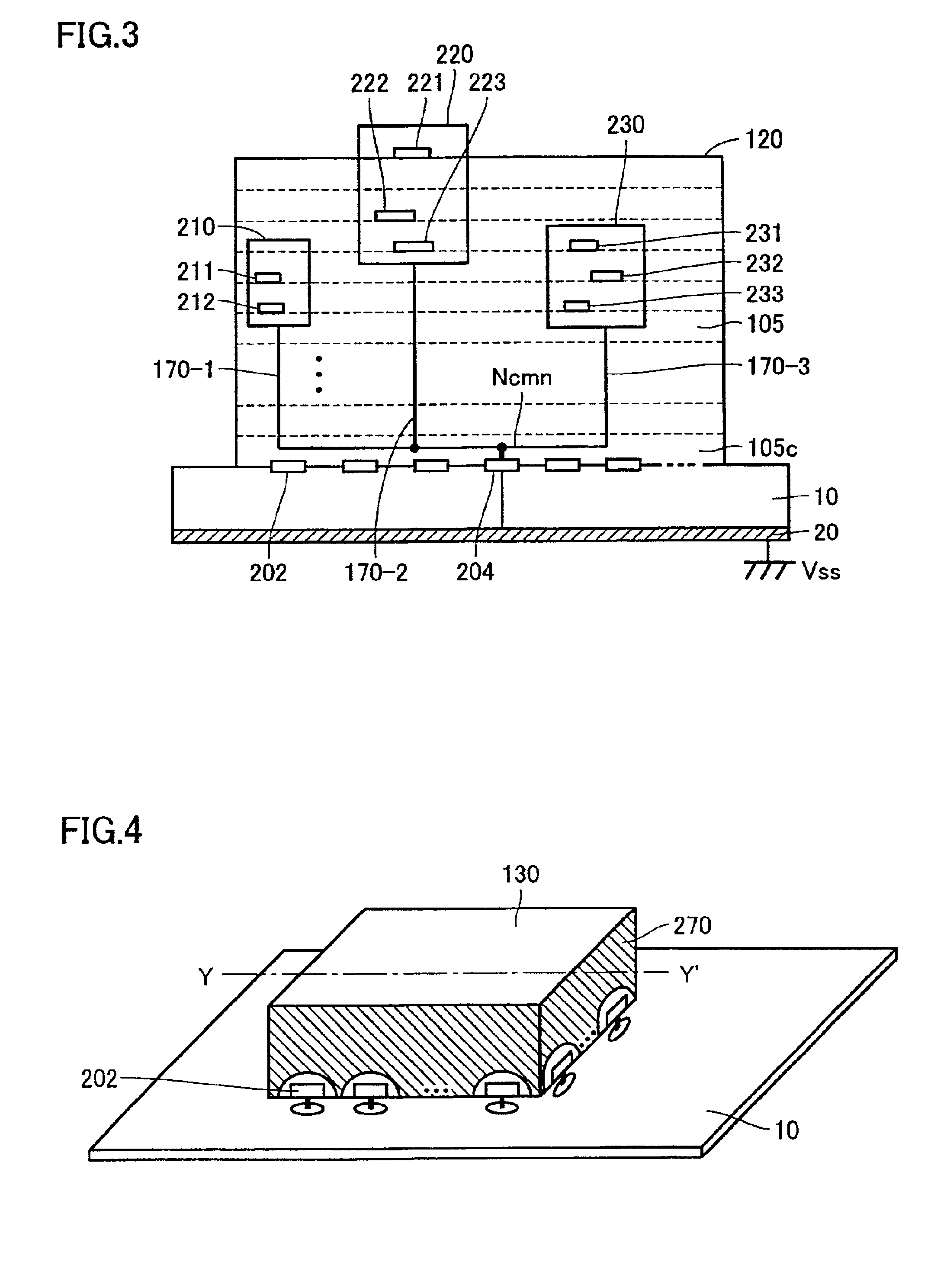
[0089]Referring to FIG. 3, a multi-layer substrate module 120 according to the second embodiment of the present invention includes a plurality of internal circuits 210, 220, 230 as in the case of the multi-layer substrate module 110 according to the first embodiment of the present invention. Since the structure and the number of internal circuits are the same as those described in the first embodiment, description thereof will not be repeated.

[0090]In the first embodiment of the present invention, ground pin terminals are respectively provided for a plurality of internal circuits. Accordingly, the ground pin terminals corresponding to the number of internal circuits are required, resulting in an increased number of pins. Therefore, in the multi-layer substrate module 120, a common node Ncmn for integrating the ground lines provided for the respective internal circuits is formed in the insulating layer 105C, so that only the common node is coupled to the grou...

third embodiment

[0094](Third Embodiment)

[0095]Referring to FIG. 4, a multi-layer substrate module 130 according to the third embodiment of the present invention is different from the multi-layer substrate module 110 of the first embodiment shown in FIG. 1 in that the multi-layer substrate module 130 includes a metal coating film 270 formed on its outer surface (side surface) so as to be connected to the earth node 20. The metal coating film 270 is electrically coupled to the earth node 20, and serves as a ground electrode. The metal coating film 270 is not formed in the regions around the pin terminals 202 other than the earth terminal 204 so that the pin terminals 202 do not contact the metal coating film 270.

[0096]Referring to FIG. 5, the multi-layer substrate module 130 according to the third embodiment of the present invention includes a plurality of internal circuits 210, 220, 230 as in the case of the multi-layer substrate module 110 according to the first embodiment of the present invention....


PUM


Abstract

In a multi-layer substrate module receiving from an external earth node supply of a reference potential for grounding, a plurality of ground lines are provided respectively corresponding to a plurality of internal circuits. Moreover, a common node for coupling the ground lines is provided in an insulating layer of the multi-layer substrate module. The common node is electrically coupled to the earth node through a ground pin terminal shared by the plurality of internal circuits. Preferably, the common node is provided in the lowest insulating layer of the multi-layer substrate module. Thus, parasitic inductance of the portion through which an earth current flows, that is, the portion common to the plurality of internal circuits, can be suppressed with a small number of ground pin terminals. Accordingly, the inflow phenomenon of the earth current between the plurality of internal circuits is prevented, enabling stable operation.

Description

TECHNICAL FIELD[0001]The present invention relates to a multi-layer substrate module, and more particularly, relates to a multi-layer substrate module on which electronic circuits operating in a high frequency range are formed, and a wireless terminal device including circuits mounted on such a multi-layer substrate module.BACKGROUND ART[0002]In recent years, electronic equipments are increasingly reduced in size and weight. According to this trend, reduction in size, weight and thickness as well as compounding are increasingly realized for the circuit substrates for use in such electronic equipments. In particular, high-frequency wireless communication devices including mobile phones utilize a multi-layer substrate using ceramics, based on, e.g., the excellent dielectric characteristics of the ceramics and the multi-layer technology. Recently, such a multi-layer substrate is increasingly reduced in size and thickness.[0003]An electronic circuit group forming the electronic equipmen...

Claims


Application Information

Patent Timeline
IPC IPC(8): H01L23/50H01L23/538H01L23/52H01L23/58H01L23/64H01L23/66H01L23/48H01L23/552H05K9/00H05K1/18H05K1/02H03H7/01H03H3/00H05K1/00H05K1/14
CPCH01L23/50H01L23/5383H01L23/552H01L23/645H05K1/0216H05K9/0039H01L2924/0002H01L2924/15312H01L2924/3011H03H3/00H03H7/01H05K1/0237H05K1/0298H05K1/141H05K2201/0715H05K2201/09254H05K2201/09972H01L2924/00
Inventor KATSURA, TAKATOSHIITOH, KENJINAGANO, HIROAKIISOTA, YOUJISHIMOZAWA, MITSUHIROTAKAGI, TADASHISUEMATSU, NORIHARUONO, MASAYOSHIMAEDA, KENICHI
Owner MITSUBISHI ELECTRIC CORP
Why Eureka
Try Eureka