Flexible sensor package responsive to thermally induced distortion

a flexible and thermally induced technology, applied in the field of sensor packages, can solve the problems of increased cost of fabricating the sensor package, adverse effect on the movement of the semiconductor sensor chip, etc., and achieve the effect of suppressing the distortion, and reducing the cost of manufacturing

Inactive Publication Date: 2005-06-14
MATSUSHITA ELECTRIC WORKS LTD
View PDF11 Cites 15 Cited by
  • Summary
  • Abstract
  • Description
  • Claims
  • Application Information

AI Technical Summary

Benefits of technology

[0005]In view of the above problems, the object of the present invention is to provide a sensor package which can prevent the climbing of the die bonding paste and can help easy positioning of the semiconductor sensor chip, as well as can prevent a distortion caused by a deformation of a printed board from reaching the semiconductor sensor chip.

Problems solved by technology

Furthermore, it can be thought that the grooves buffer a distortion caused by the deformation of the printed board and make it difficult for the distortion to reach the semiconductor sensor chip so that a device carrying the sensor package can be prevented from introducing a malfunction due to an unnecessary distortion added to the semiconductor sensor chip.
On this occasion, if the die bonding paste has been applied superfluously, the die bonding paste may climb the semiconductor sensor chip when the sensor chip is laid on the bottom wall and have an adverse effect on movement of the semiconductor sensor chip.
Furthermore, in order to monitor the location by means of the CCD camera, a certain mark must be formed, which results in increased costs for fabricating the sensor package.
As mentioned above, prior sensor packages can prevent the distortion caused by the deformation of the printed board from reaching the semiconductor sensor chip, but still have problems related to prevention of the climbing of the die bonding paste and improvement in the positioning of the semiconductor sensor chip.

Method used


Image

  • Flexible sensor package responsive to thermally induced distortion
  • Flexible sensor package responsive to thermally induced distortion
  • Flexible sensor package responsive to thermally induced distortion

Examples


second embodiment

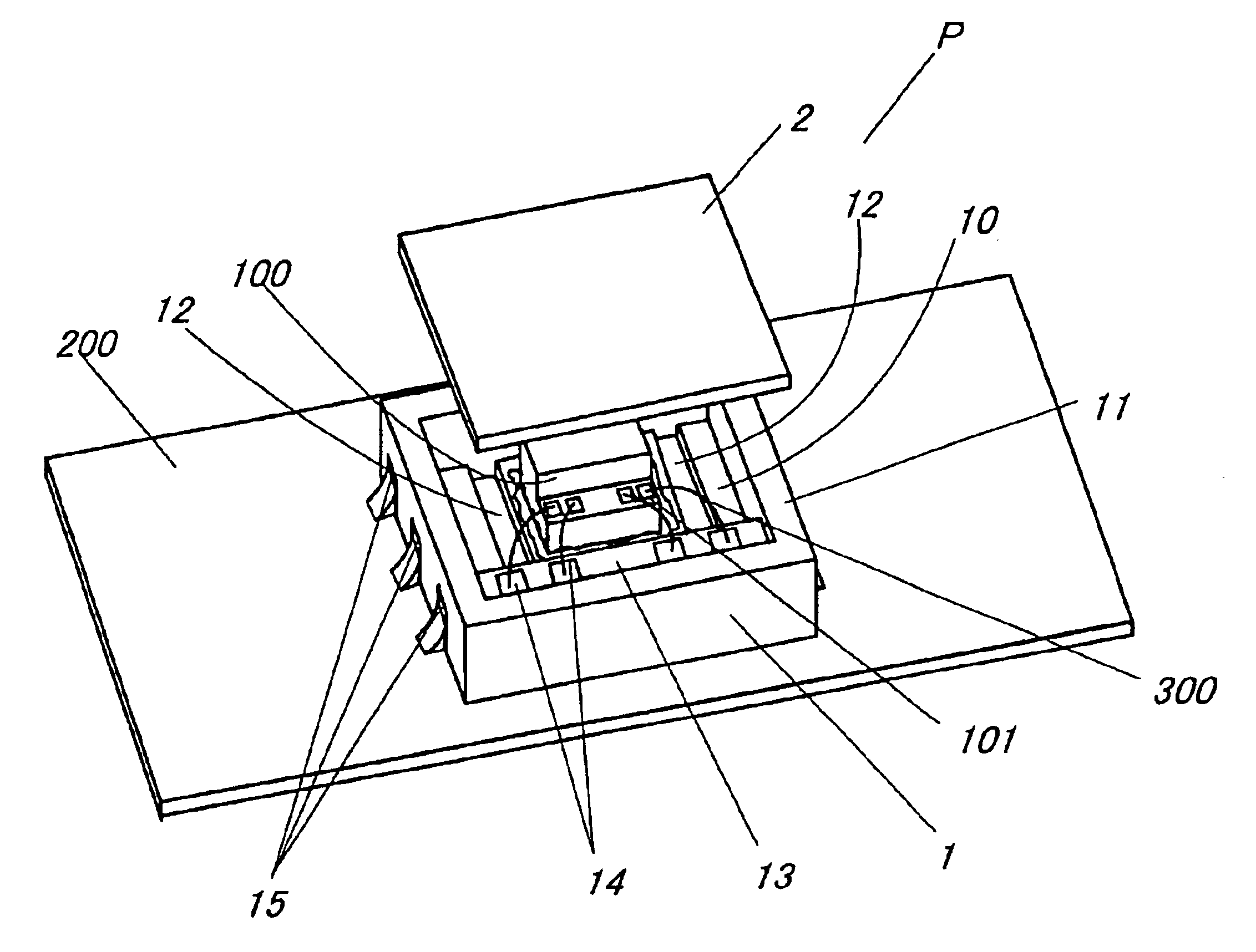
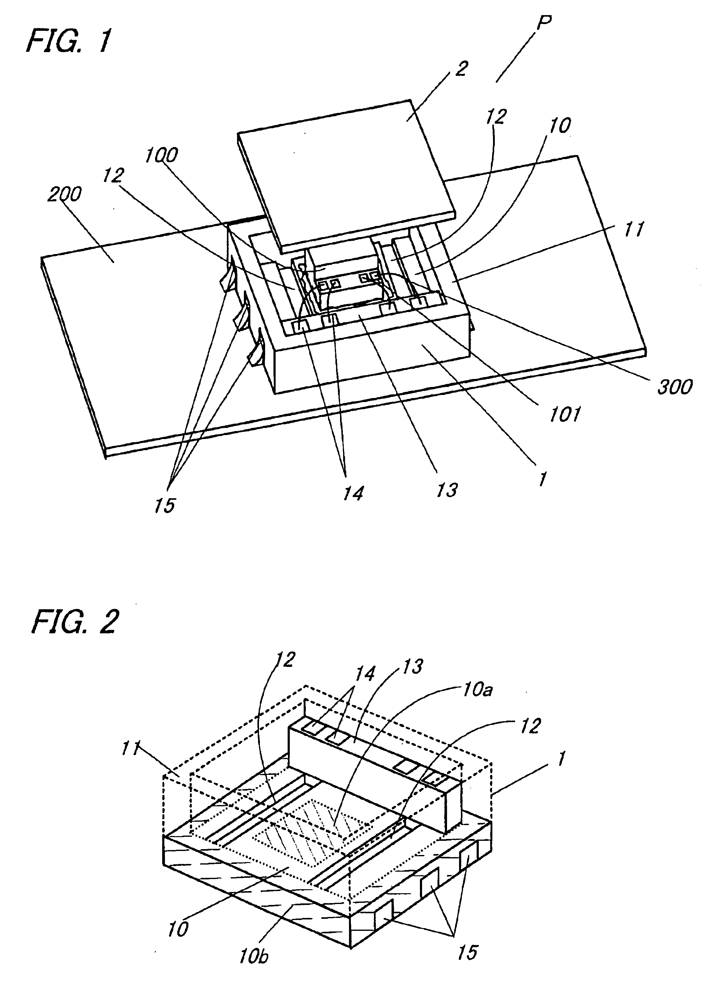
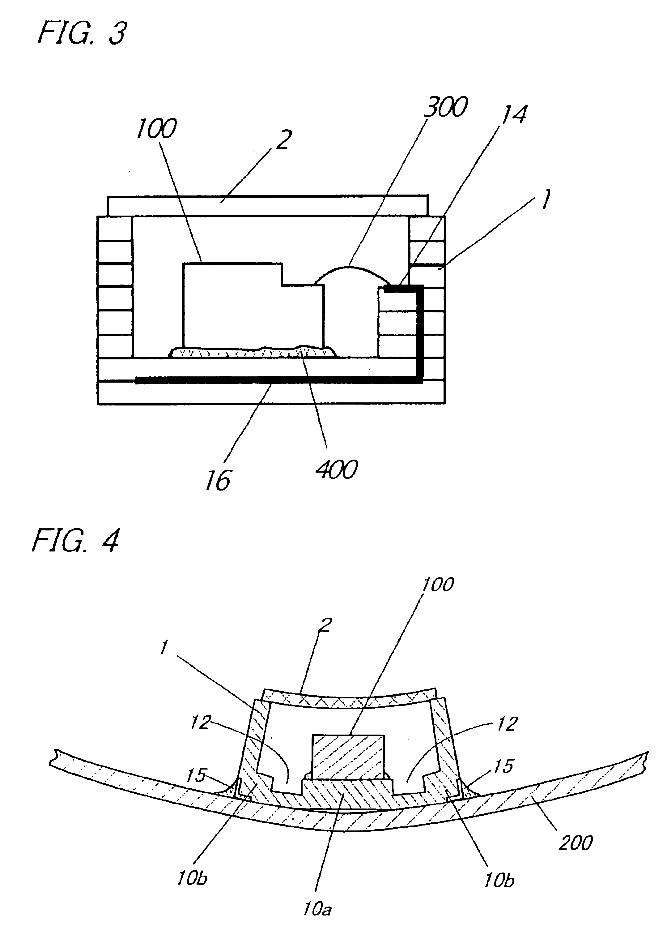
[0045]FIG. 10 shows a sensor package P1 in accordance with the present invention. This sensor package P1 is provided with a recess 20 formed in an interior surface of the center area 10a on which the semiconductor acceleration sensor chip 100 is mounted, in addition to the above construction of the sensor package P. The recess 20 is shaped into a rectangle in the interior surface and forms a support flange 21 around the recess for supporting the bottom of the semiconductor acceleration sensor chip 100. As shown in FIG. 11, the recess is filled with an elastic connective agent 22, for example, a die bonding agent of silicon series such as silicone resin, and an entire circumference of the bottom of the semiconductor acceleration sensor chip 100 is laid on the support flange 21.

[0046]By providing the recess 20, a contact area between the center area 10a and the semiconductor acceleration sensor chip 100 can be decreased, so that the distortion will have more difficulty in reaching the...

third embodiment

[0050]FIG. 17 shows a sensor package P2 in accordance with the present invention. This sensor package P2 is provided with support legs 30 on the outer bottom of the peripheral area 10b, in addition to the above construction of the sensor package P. The support legs 30 are formed along two opposite sides of the outer bottom of the peripheral area 10b which are parallel to the grooves 12. The output electrodes 15 are formed in U-shaped configuration which straddles a bottom face and both side faces of the support leg 30.

[0051]In such a sensor package P2, by providing the support legs 30, a deflection along the longitudinal direction of the printed board 200 can be suppressed by a deformation of the support legs 30 in addition to the deformation of the peripheral area 10b outside the grooves 12, so that the deflection of the printed board 200 will have more difficulty in reaching the semiconductor acceleration sensor chip 100. Furthermore, even if there is not enough space for the groo...


PUM


Abstract

A sensor package P is a surface-mounted sensor package which is adapted to be mounted on a printed board 200. The sensor package P includes a case 1 for accommodating a semiconductor acceleration sensor chip 100 having output pads 101. The case has a bottom wall 10, which is divided into a center area 10a for supporting the sensor chip 100 and a peripheral area 10b. Output electrodes 15 to be connected to the output pads 101 are formed on external surfaces of the peripheral area. These output electrodes 15 are soldered to the printed board 200 for electrical connection between the sensor chip and an electric circuit of the printed board as well as for holding the sensor package physically on the printed board. The feature of the present invention resides in that grooves 12 are formed in an interior surface of the bottom wall 10 between the center area 10a and the peripheral area 10b.

Description

TECHNICAL FIELD[0001]This invention relates to a sensor package for accommodating a semiconductor sensor chip.BACKGROUND ART[0002]Japanese Non-examined Patent Publication No.11-260960 discloses a sensor package for accommodating a semiconductor sensor chip such as a semiconductor acceleration sensor chip. This sensor package is a type of surface-mounted package and is adapted to be mounted on a surface of a printed board. This sensor package comprises a case for accommodating the semiconductor sensor chip and output electrodes provided on an undersurface of the case. The output electrodes are soldered to a printed board for connecting the semiconductor sensor chip electrically to an electric circuit of the printed board as well as for holding the sensor package physically on the printed board. The case has a bottom wall for fixing the semiconductor sensor chip on its upper surface. The output electrodes are formed in the undersurface of the bottom wall. A plurality of concave groove...

Claims


Application Information

Patent Timeline
Patent Type & Authority Patents(United States)
IPC IPC(8): G01P1/02G01P1/00H05K3/34G01P15/08G01P15/125H01L29/84
CPCB81B7/0048G01P15/0802G01P15/125G01P1/023B81B2201/0235B81C2203/032H05K3/3442H01L24/32H01L2224/05554H01L2224/26175H01L2224/48091H01L2224/48227H01L2224/49171H01L2224/73265H01L2224/83385H01L2924/15153H01L2924/16195H01L2924/3511H01L2924/00014H01L23/04
Inventor FURUKUBO, EIICHIHORI, MASAMINOHARA, KAZUYA
Owner MATSUSHITA ELECTRIC WORKS LTD
Why Eureka
Try Eureka