Digital to analog converter with a weighted capacitive circuit

a capacitive circuit and digital converter technology, applied in the field of d/a converters, can solve the problems of deteriorating integral linearity, difficulty of convertor, and variation in resistance value, and achieves the effects of small area, high precision, and simple structure and operation

Inactive Publication Date: 2005-06-14
LINEAR CELL DESIGN COJ
View PDF13 Cites 95 Cited by
  • Summary
  • Abstract
  • Description
  • Claims
  • Application Information

AI Technical Summary

Benefits of technology

[0013]A first object of the present invention is to realize a D/A converter that does not receive influence of an error caused by a parasitic capacitance, which has been a significant problem in a conventional charge-scaling type D/A converter, by using a simple structure and operation, and to provide a D/A converter with a small area but with high precision. A second object of the present invention is to provide a D/A converter having no offset error without receiving influence of the offset voltage of an internal buffer, or the like, that is required to obtain amplified output. A thi...

Problems solved by technology

However, this converter has difficulty in the fact that, in a high bit, variation in the value of resistance deteriorates integral linearity.
However, since the input capacitance of a buffer and the parasitic capacitance Cp by the switch SWR5 exist in the node N1 of FIG. 15 in practice, an electric charge is distributed to this parasitic capacitance, and, as a result, an error occurs.
If the parasitic capacitance Cp has voltage dependence, the linearity of the D/...

Method used


Image

  • Digital to analog converter with a weighted capacitive circuit
  • Digital to analog converter with a weighted capacitive circuit
  • Digital to analog converter with a weighted capacitive circuit

Examples


first embodiment

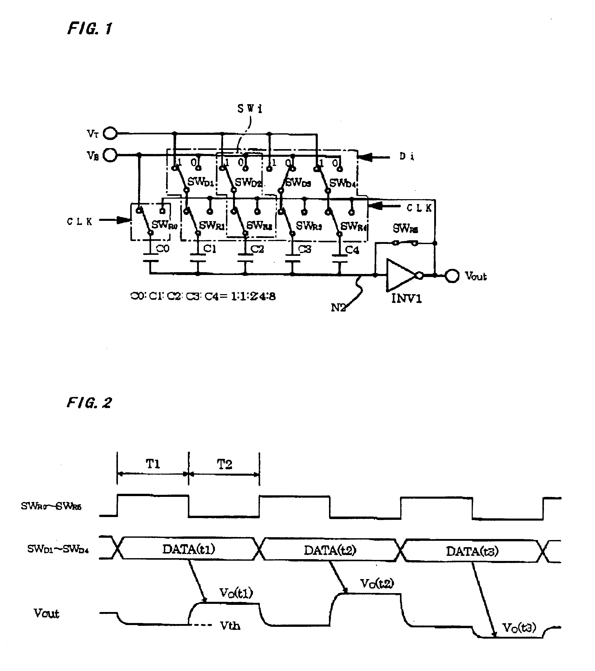
[0045]FIG. 1 is a 4-bit D / A converter shown as a first embodiment to explain the basic operation of the present invention. In FIG. 1, capacitors C1 to C4 are binary-weighted capacitors the capacitance-value ratio of which is 1:2:4:8, and capacitor C0 is a terminating capacitor the capacitance-value ratio of which is 1. One end of each of these capacitors C0 to C4 is connected in common to an input node N1 of an inverting amplifier (INV1). The other end of each of the capacitors C1 to C4 is independently connected to either of a bottom reference voltage VB and a top reference voltage VT that serves as two main reference voltages in the reset operation, and is connected to switches SWR0 to SWR4 that are connected in common to an output of the inverting amplifier INV1 in the output operation. In the binary-weighted capacitors C1 to C4, the main reference voltage connected to each capacitor is selectively given by the switches SWD1 to SWD4 controlled on the basis of digital data, and, i...

second embodiment

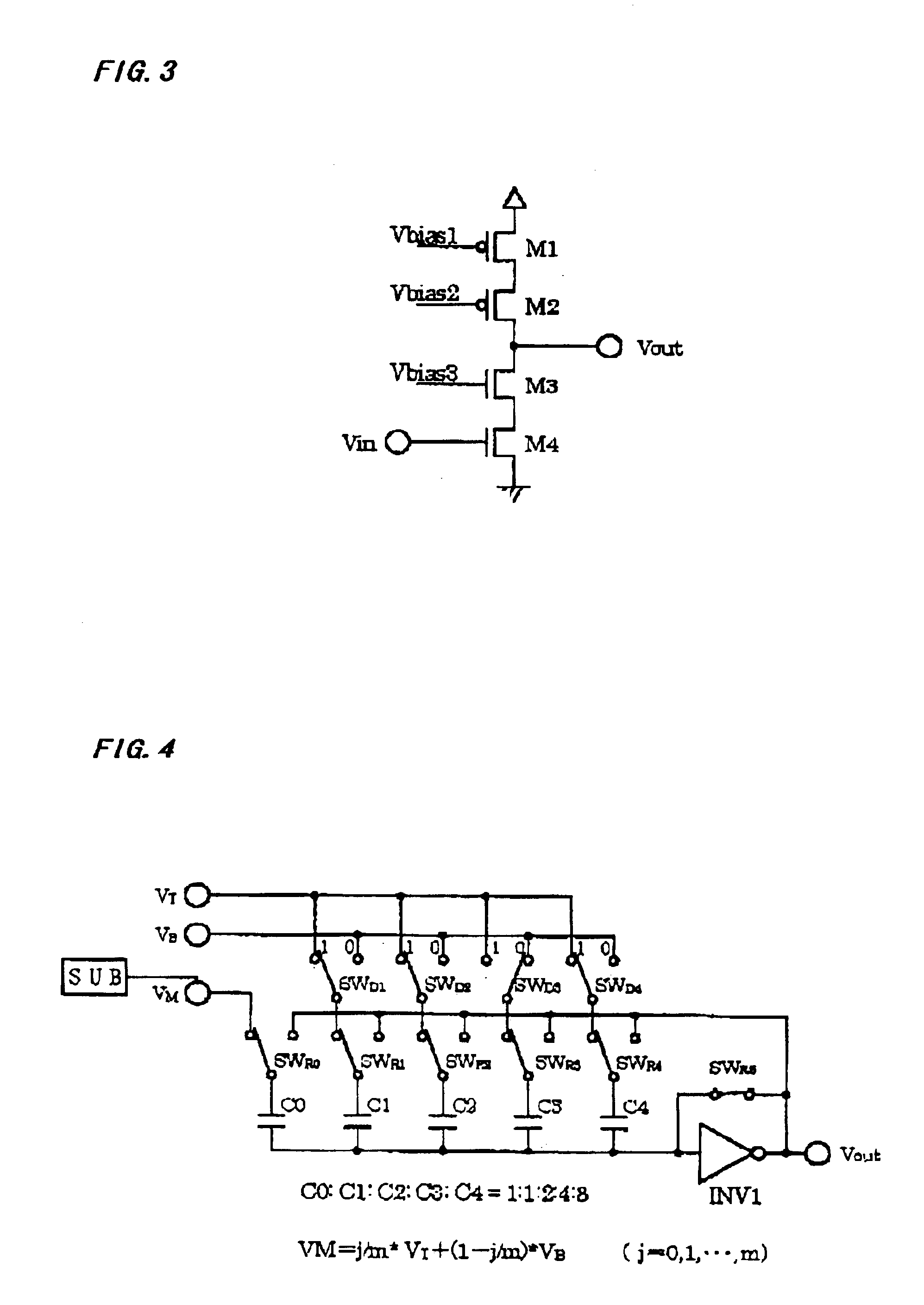
[0055]Next, referring to FIG. 4, a description will be given of a method of realizing a D / A converter with a small circuit size even when the resolution is increased in the present invention. Normally, when the intention is accomplished to obtain n-bit resolution by using the conventional structure of FIG. 15 or the structure of the present invention of FIG. 1, the full capacitor size with respect to the unit capacitor is 2n because the ratio of required binary-weighted capacitors is 1:2:4: . . . :2(n−1). This is, for example, 256 in 8 bits and is 1024 in 10 bits which become exponentially great, and an extremely large circuit area is required for a high-resolution D / A converter. A method for solving this problem is shown in FIG. 4.

[0056]The structure of FIG. 4 is exactly identical to that of FIG. 1 except for the voltage given to the terminating capacitor C0, and is made up of an inverting amplifier (INV1), a feedback switch SWR5 provided between the input and output of the inverti...

third embodiment

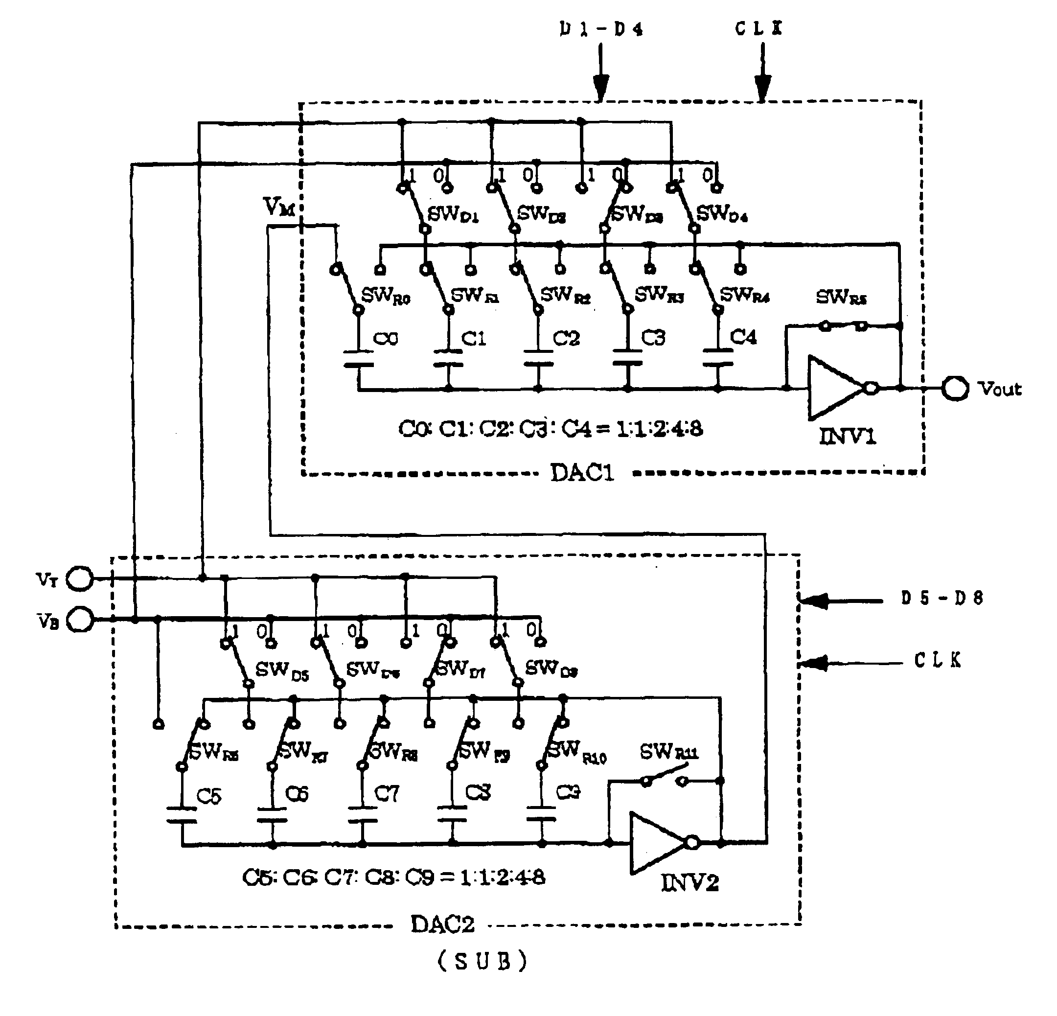
[0060]Next, referring to FIG. 5, a description will be given of a third embodiment formed as a more concrete structure based on the second embodiment shown in FIG. 4. In the foregoing description, it has been mentioned that the sub-reference voltage can be generated by a string of a plurality of resistors in series. However, the capacitor can obtain higher precision than the resistor in a CMOS process. FIG. 5 shows an 8-bit D / A converter realized by adding a D / A converter having the same structure as that of FIG. 1 as a sub reference voltage generating circuit SUB and by combining two 4-bit D / A converters together so that the precision of the sub-reference voltage can be determined by a capacitance-value ratio without using the resistor string.

[0061]In FIG. 5, DAC2 is a 4-bit D / A converter having the same structure as that of FIG. 1, and is made up of an inverting amplifier INV2, a feedback switch SWR11 provided between the input and output of the inverting amplifier INV2, binary-we...


PUM


Abstract

D/A converter of this invention including n+1 capacitors in total consisting of one terminating capacitor (C0) and n binary-weighted capacitors (C1-4) that are subjected to binary weighting ratio of 1:2:4: . . . :2(n−1), and, an inverting amplifier (INV1), further comprising: a feedback switching means (SWR5) provided between the input and output of the inverting amplifier (INV1); a switching means for terminating operation (SWR0) supplies one of two main reference voltages (VB,VT) to the terminating capacitor (C0), and then, makes connection of the terminating capacitor (C0) to the output of the inverting amplifier (INV1); a plurality of switching means for input operation (SWD1-4,SWR1-4) makes selection of one of the two main reference voltages (VB,VT) to be provided for the n binary-weighted capacitors (C1-4) depending on digital data (D1-4), and then, makes connection of the second terminal side of the n binary-weighted capacitors (C1-4) to the output of the inverting amplifier (INV1).

Description

CROSS-REFERENCE TO RELATED APPLICATIONS[0001]This patent application is a continuation-in-part application of copending U.S. patent application Ser. No. 09 / 982,303, filed on Oct. 17, 2001, now U.S. Pat. No. 6,611,164, the right of priority of which is hereby claimed for this application. This patent application is also related to Japanese Patent Application Serial No. 2000-317998, filed on Oct. 18, 2000 and to Japanese Patent Application Serial No. 2002-107583, filed on Apr. 10, 2002, the rights of priority of which are also hereby claimed for this application.TECHNICAL FIELD[0002]The present invention relates to a D / A converter that converts digital data into an analog voltage, and in particular, to a D / A converter that uses a weighted capacitive circuit on a CMOS device capable of obtaining high-resolution output with a small area.BACKGROUND ART[0003]In order to realize a D / A converter on a CMOS device, general use is made of a voltage-scaling type D / A converter in which a plurali...

Claims


Application Information

Patent Timeline
IPC IPC(8): G06G7/14G06G7/00H03M1/80H03M1/74H03M1/06H03M1/68
CPCG06G7/14H03M1/804H03M1/68H03M1/0682
Inventor UNO, MASAYUKI
Owner LINEAR CELL DESIGN COJ
Why Eureka
Try Eureka