
Integrated DRAM semiconductor memory and method for operating the same

a technology of integrated dram and semiconductor memory, applied in information storage, static storage, digital storage, etc., can solve the problems of high susceptibility, weak enough to generate a sufficient differential signal, and incorrect evaluation of secondary sense amplifiers, so as to reduce the dependence on individual mdq switches

Inactive Publication Date: 2005-06-14
QIMONDA
View PDF4 Cites 7 Cited by
  • Summary
  • Abstract
  • Description
  • Claims
  • Application Information

AI Technical Summary

Benefits of technology

[0011]An integrated semiconductor memory, in particular DRAM memory of the generic type, and a method for operating the same are described in that general pre-charge performance of the main data lines MDQ and of the local data lines LDQ is improved, and the dependence on the individual MDQ switches decreases.
[0015]What is achieved by the connection of the local data lines of at least two adjacent LDQ segments to the LDQ switch is that, in the precharge phase, the local data line of an LDQ segment is precharged (precharge) via at least two instead of one MDQ switch. Since the adjacent LDQ segments have already been in precharge for longer, they support the charge equalization and thus alleviate the read access—which is critical with regard to the precharge time—to the same LDQ segment with inverted data relative to the preceding write command.

Problems solved by technology

However, assuming inverted (logical) data between write and read commands, this can have the effect that the signal on the bit line BLT, BLC that is switched on to the local data lines LDQT and LDQC during the read operation by the primary sense amplifier 1 via the CSL switch 3 is not strong enough to generate a sufficient differential signal on the complementary local data lines LDQT, LDQC.
This can lead to an incorrect evaluation of the secondary sense amplifier.
What is problematic in this case is primarily the fact that only one MDQ switch 5 is used per LDQ segment in order to switch through the LDQ precharge.
This results in a high susceptibility which causes the semiconductor memory module to fail beyond the repair limit.

Method used


Image

  • Integrated DRAM semiconductor memory and method for operating the same
  • Integrated DRAM semiconductor memory and method for operating the same
  • Integrated DRAM semiconductor memory and method for operating the same

Examples


Embodiment Construction

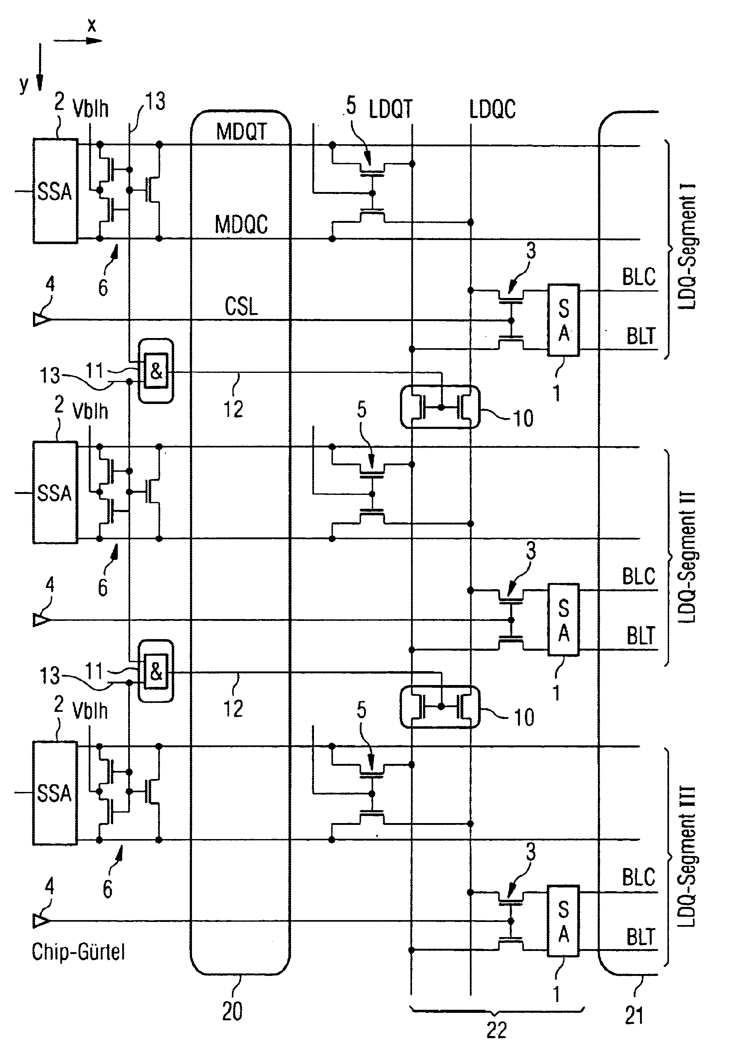
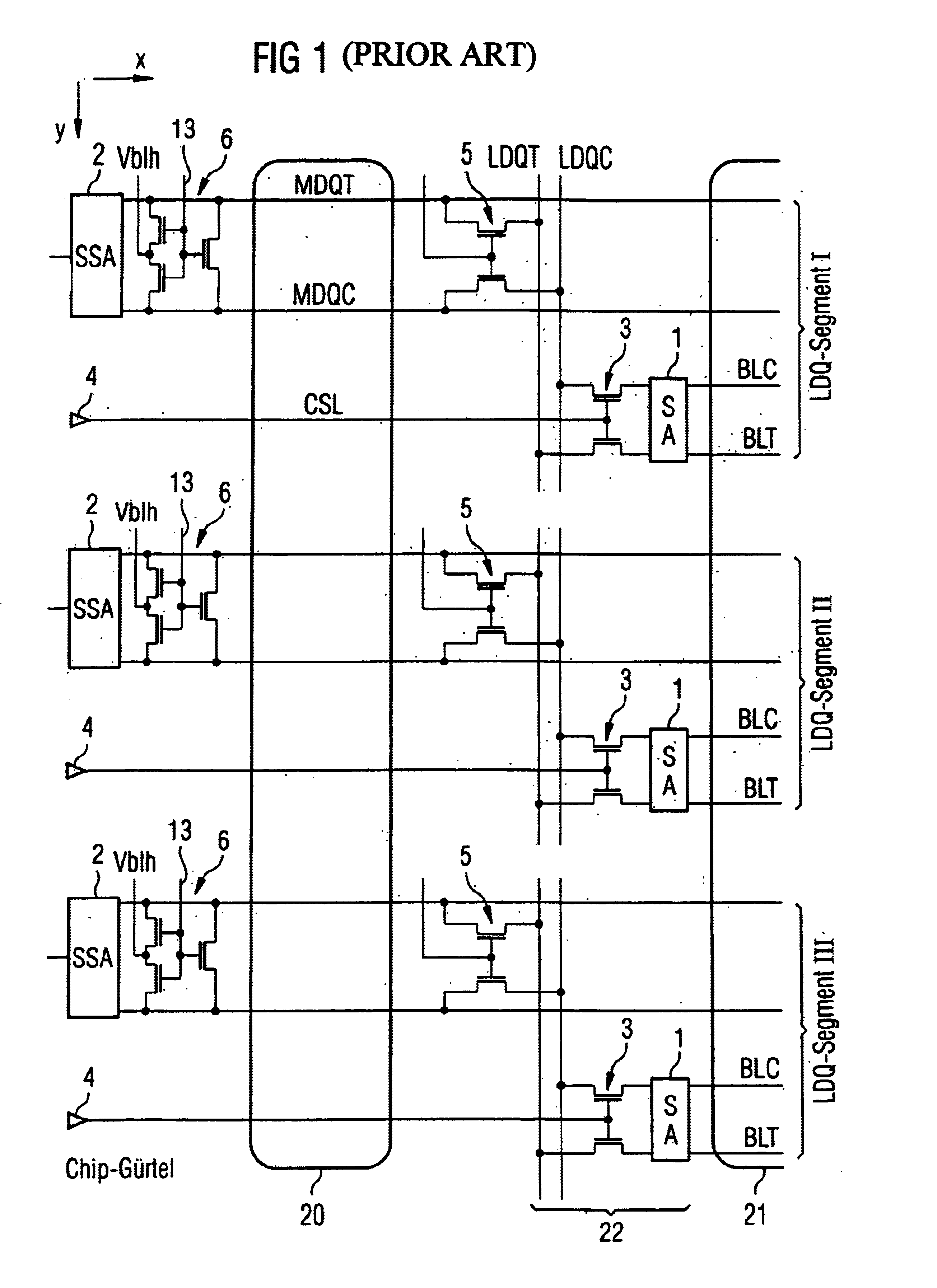
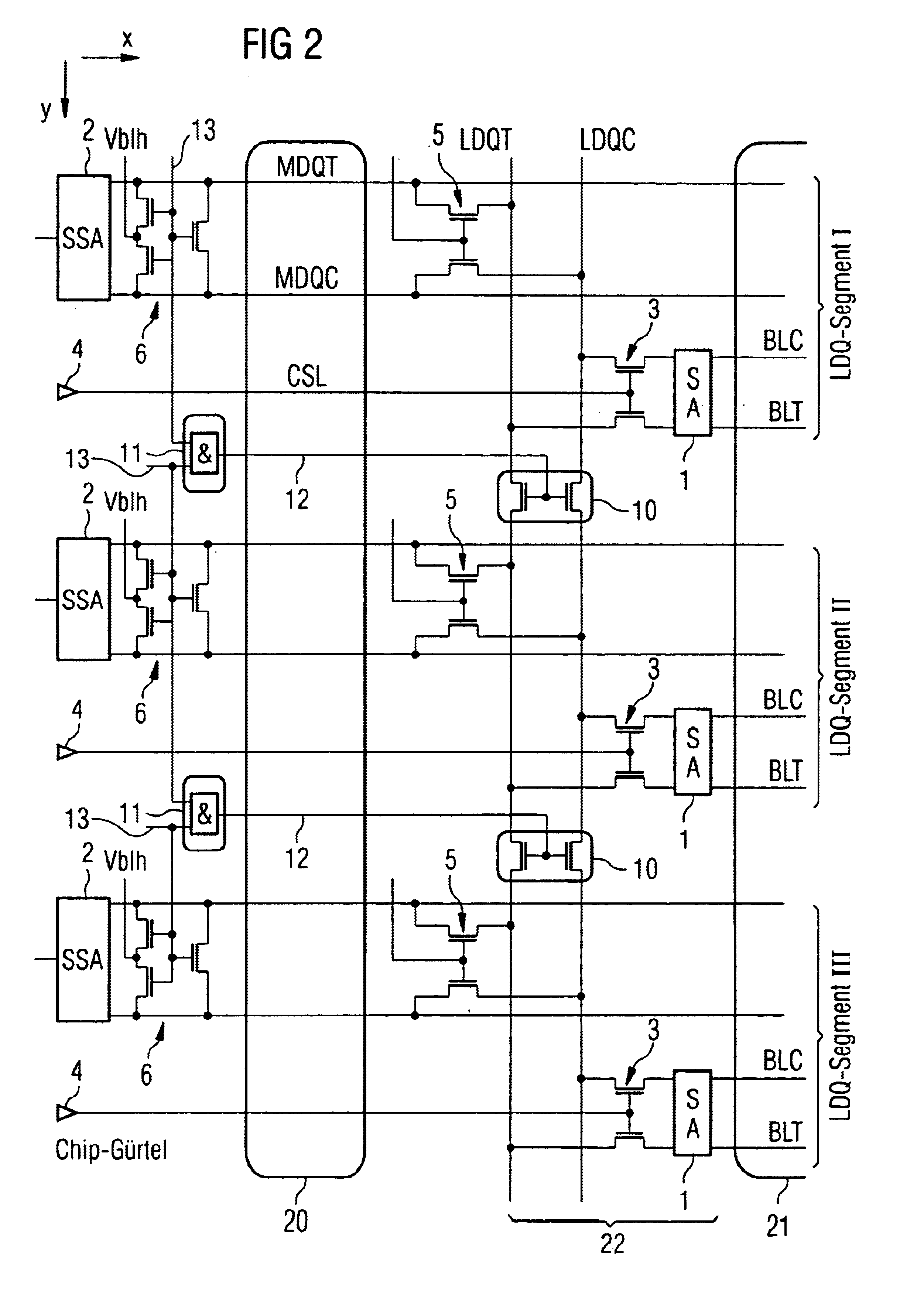
[0021]The following reference symbols are used in the connection with the following description:[0022]1 Sense amplifier SA[0023]2 Secondary sense amplifier SSA[0024]3 CSL switch[0025]4 CSL driver[0026]5 MDQ switch[0027]6 EQL control circuit[0028]10 LDQ switch[0029]11 AND elements[0030]12 LDQ switch control line[0031]13 Precharge control signals[0032]20, 21 Cell blocks[0033]22 SA strips[0034]BLT, BLC Bit lines[0035]LDQT, LDQC Local data lines[0036]MDQT, MDQC Main data lines[0037]CSL Column select line[0038]Vblh Full bit line voltage[0039]L New precharge charging function[0040]X Row Direction[0041]Y Column direction[0042]I, II, III LDQ segments

[0043]A DRAM semiconductor memory and method for operating the same is disclosed in U.S. Pat. No. 2002 / 0067653 A1, the disclosure of which is incorporated by reference in its entirety.

[0044]In FIG. 2, which shows, schematically and partly as a block diagram, a section of a DRAM memory configured in accordance with an embodiment of the invention,...


PUM


Abstract

An integrated semiconductor memory, and method for operating such a memory, in particular a DRAM memory, having local data lines (LDQT, LDQC) segmented in the column direction (Y), which local data lines can be connected by a CSL switch in response to a column select signal fed via a CSL line (CSL) running in the row direction (X) to primary sense amplifiers for transferring or accepting spread data signals to or from bit lines of the respective segment (I, II, III), LDQ switches are arranged at the interfaces between adjacent segments of the local data lines (LDQT, LDQC) for their connection to the local data lines (LDQT, LDQC) of adjacent segments (I, II, III). LDQ switches, depending on a control signal fed separately to each of said LDQ switches, are closed during a precharge phase, which takes place before each read cycle, of at least two adjacent LDQ segments.

Description

BACKGROUND[0001]1. Field of the Invention[0002]The present invention relates to an integrated DRAM semiconductor memory and a method for operating the same.[0003]2. Background Information[0004]In a read cycle for integrated semiconductor memories, such as dynamic memory modules (DRAMs), in order to transport the evaluated bit line levels to the chip output, the bit line signals spread by a primary sense amplifier are switched onto local data lines (LDQs) via CSL switches in a first stage. For power-saving reasons, and in order that the primary sense amplifier that spreads the bit lines BL can drive the bit line signals within a short time on the LDQ, the capacitance of the LDQs that is to be subjected to charge reversal is usually reduced by segmentation or division of the same.[0005]FIG. 1 shows a section of a cell array of a conventional DRAM memory with two cell blocks 20, 21. Situated between the two cell blocks is a SA strip 22, in which the above-mentioned primary sense amplif...

Claims


Application Information

Patent Timeline
Patent Type & Authority Patents(United States)
IPC IPC(8): G11C11/4096G11C7/10G11C11/4091G11C11/409
CPCG11C7/1048G11C7/1051G11C11/4091G11C11/4096G11C7/1069G11C2207/002
Inventor PROELL, MANFREDSCHROEDER, STEPHANSCHNEIDER, RALFKLIEWER, JOERG
Owner QIMONDA
Learn More