CT detector with integrated air gap

a detector and air gap technology, applied in the field of diagnostic imaging, can solve the problems of detector replacement and downtime, catastrophic failure of ct detector, and known opti-couplers that are susceptible to cracking or breaking away from scintillator and/or photodiode array, so as to improve the light absorption efficiency and improve the light collection efficiency of photodiodes.

Inactive Publication Date: 2005-06-14
GENERAL ELECTRIC CO
View PDF4 Cites 57 Cited by
  • Summary
  • Abstract
  • Description
  • Claims
  • Application Information

AI Technical Summary

Benefits of technology

[0008]The present invention is directed to an improved CT detector scintillator to photodiode optical coupling that overcomes the aforementioned drawbacks. The CT detector utilizes a controlled air gap between the photodiode array and the scintillator array together with an anti-reflective layer on the scintillator array. To improve the absorption of light at the photodiode array, the photodiode array includes a textured light reception surface. By incorporating a textured layer with the photodiode array, the light collection efficiency of the photodiodes is improved. The textured layer may extend along an x and / or z-axis and the texturing may be in different forms. For example, the textured layer may include a series of pyramidally-shaped protrusions.

Problems solved by technology

Despite these advancements, known opti-couplers remain susceptible to cracking or breaking away from the scintillator and / or photodiode array.
This premature cracking or breaking away can result in catastrophic failure of the CT detector thereby warranting full detector replacement and downtime of the CT system.

Method used


Image

  • CT detector with integrated air gap
  • CT detector with integrated air gap
  • CT detector with integrated air gap

Examples


Embodiment Construction

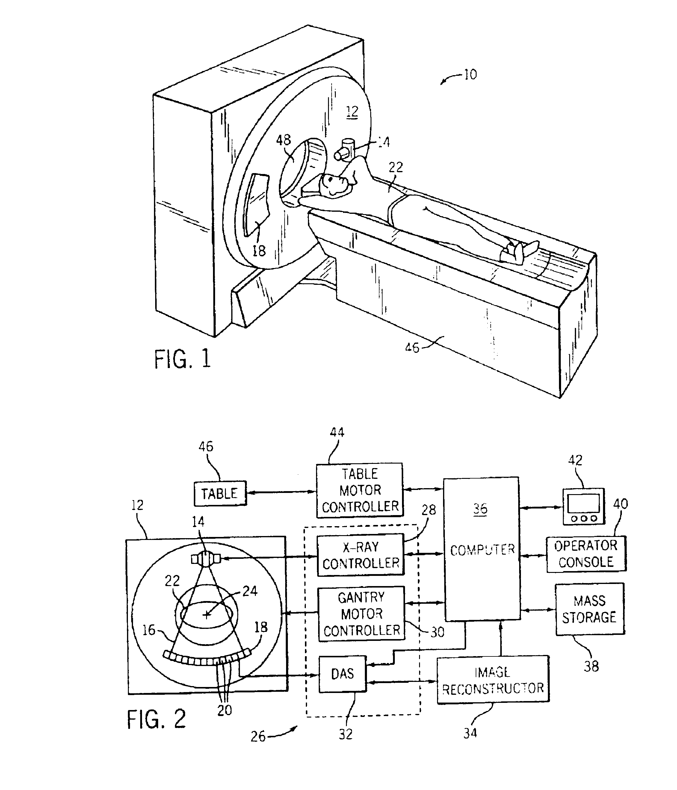
[0024]The operating environment of the present invention is described with respect to a four-slice computed tomography (CT) system. However, it will be appreciated by those skilled in the art that the present invention is equally applicable for use with single-slice or other multi-slice configurations. Moreover, the present invention will be described with respect to the detection and conversion of x-rays. However, one skilled in the art will further appreciate that the present invention is equally applicable for the detection and conversion of other high frequency electromagnetic energy. The present invention will be described with respect to a “third generation” CT scanner, but is equally applicable with other CT systems.

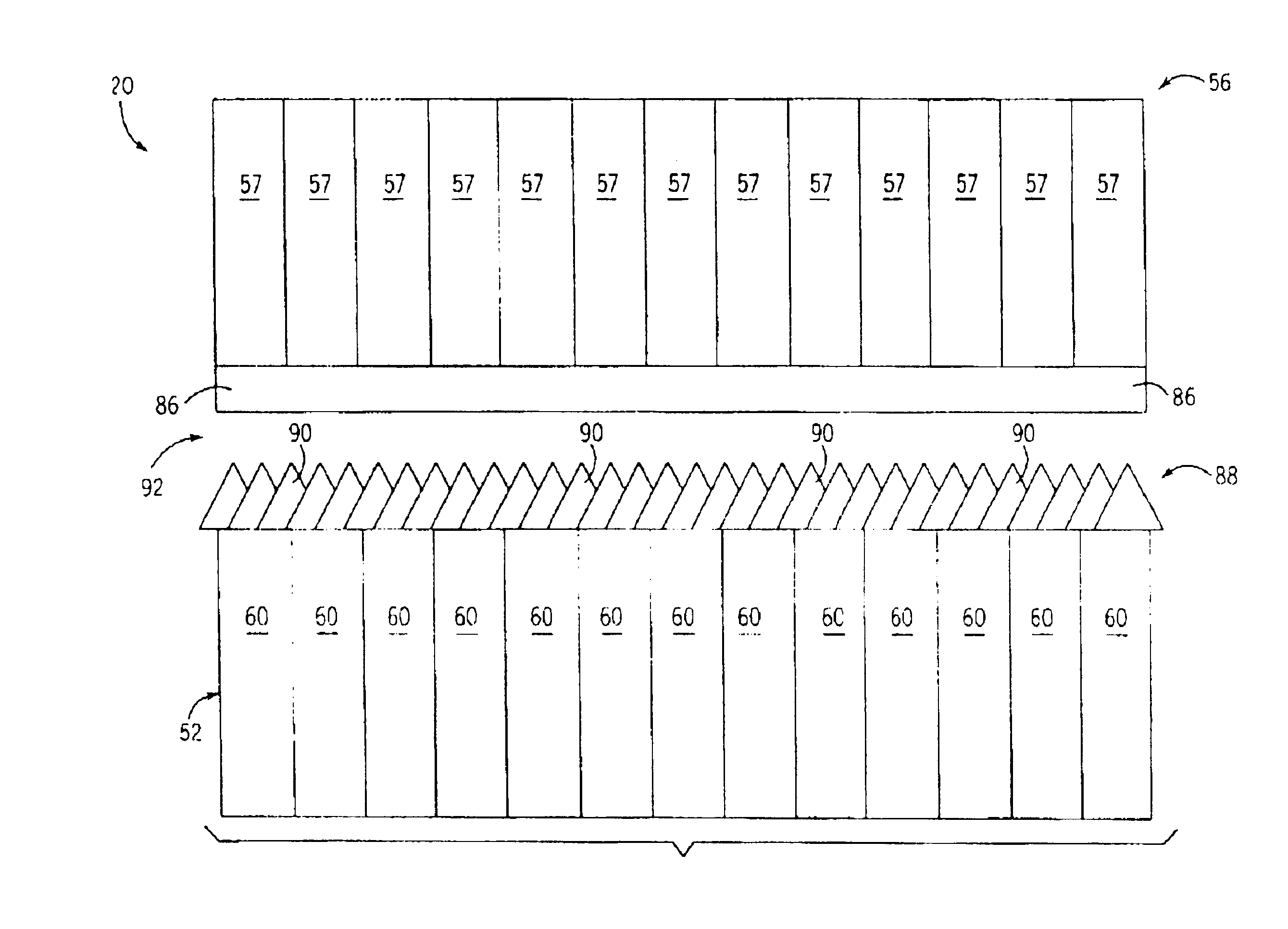
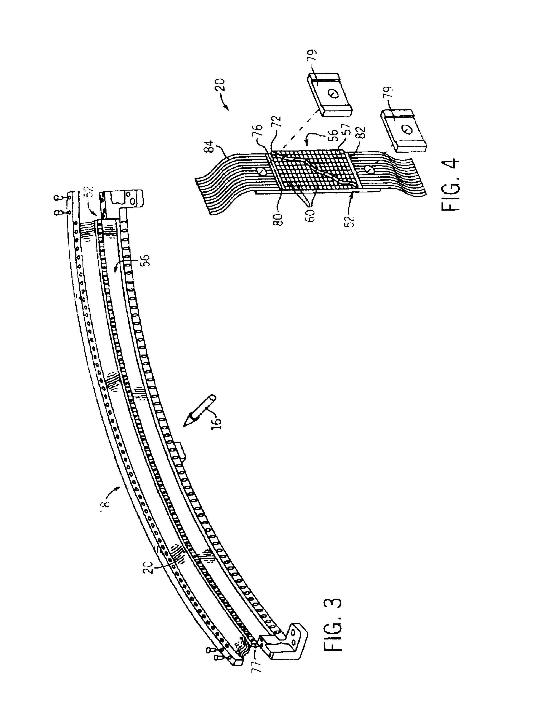
[0025]Referring to FIGS. 1 and 2, a computed tomography (CT) imaging system 10 is shown as including a gantry 12 representative of a “third generation” CT scanner. Gantry 12 has an x-ray source 14 that projects a beam of x-rays 16 toward a detector array 18 on the...


PUM

PropertyMeasurementUnit
thickaaaaaaaaaa
thickaaaaaaaaaa
widthaaaaaaaaaa

Abstract

The present invention is directed to an improved CT detector scintillator to photodiode optical coupling. The CT detector utilizes a controlled air gap between the photodiode array and the scintillator array together with an anti-reflective layer on the scintillator array. To improve the absorption of light at the photodiode array, the photodiode array includes a textured light reception surface. By incorporating a textured layer with the photodiode array, the light collection efficiency of the photodiodes is improved. The textured layer may extend along an x- and/or z-axis and the texturing may be in different forms. For example, the textured layer may include a series of pyramidally-shaped protrusions.

Description

BACKGROUND OF THE INVENTION[0001]The present invention relates generally to diagnostic imaging and, more particularly, to a CT detector with an integrated air gap. More particularly, the CT detector includes a scintillator array having an anti-reflective layer is attached to a photodiode array having a textured surface such that a controlled air gap exists therebetween.[0002]Typically, in computed tomography (CT) imaging systems, an x-ray source emits a fan-shaped beam toward a subject or object, such as a patient or a piece of luggage. Hereinafter, the terms “subject” and “object” shall include anything capable of being imaged. The beam, after being attenuated by the subject, impinges upon an array of radiation detectors. The intensity of the attenuated beam radiation received at the detector array is typically dependent upon the attenuation of the x-ray beam by the subject. Each detector element of the detector array produces a separate electrical signal indicative of the attenuat...

Claims


Application Information

Patent Timeline
Patent Type & Authority Patents(United States)
IPC IPC(8): A61B6/03A61B6/08G01N23/00G01T1/20G01T1/29G01T1/00G21K1/00G21K1/12H05G1/64H05G1/00H04N5/32
CPCG01T1/2985G01T1/2002
Inventor HOFFMAN, DAVID M.
Owner GENERAL ELECTRIC CO
Why Eureka
Try Eureka