Tailored interconnect module

a technology of interconnect modules and connectors, applied in the direction of solid-state devices, basic electric elements, semiconductor devices, etc., can solve the problems of increasing the increasing the difficulty of routing circuit board connections (traces) to pins, and increasing the risk of use, so as to facilitate a high degree of local routing and reduce the total pin count. , the effect of minimizing the total number of nodes connected to external pins

Inactive Publication Date: 2005-06-21
ALCATEL LUCENT SAS
View PDF1 Cites 72 Cited by
  • Summary
  • Abstract
  • Description
  • Claims
  • Application Information

AI Technical Summary

Benefits of technology

[0006]The present invention provides a tailored interconnect module which provides the interconnect reduction as its major objective along with functionality and design rules in place to support this. According to the invention, the interconnects on the module are configured and adapted to facilitate a high degree of local routing, i.e. the majority of the nodes on the peripheral devices are designed to interface with the nodes of one or more central devices (ASICs) processors, etc.) in such a way as to condense the number of nets so that the total number of nodes connected to external pins is minimized. The same is true for the power and ground pins of the device. Rather than simply supplying each device in question, they can be pooled to a set of local reference pins for distribution to the other devices from this central localized reference pin. In the extreme, the present invention can be leveraged to the point where all the interconnects will be contained locally and the number of pins existing the package could be reduced to as low as one directional pin. In practice, the invention can be leveraged to reduce the total pin count from 4000 pins approximately to 500 pins.
[0007]This invention integrates fully tested devices in chip scale packages into a single package, thereby trading-off intra-device performance of multi-chip modules for an improvement in manufacturing yield. The resulting reduced pin count alleviates routing constraints, which allows a circuit board with fewer layers to be used.
[0008]In most cases, only one or two high pin count devices (e.g. a network processor) dictate the number of board layers required for routing. An example application would be to integrate a network processor and its supporting memory chips into a tailored interconnect module. In this case, use of the tailored interconnect module could reduce the required circuit board layers from 35 layers to 20 layers, which would allow the circuit board to be implemented in standard circuit board technology, thereby reducing costs and improving the reliability of the board. Other applications would be to create generic tailored interconnect module components for performing common functions such as data / signal processing, supplying power, etc.
[0009]An alternative to solely using devices in chip scale packages in the tailored interconnect module would be to use a combination of packaged and bare die. This alternative could still provide the same benefits to yields and routing where the bare die could be tested at speed, i.e. where different parts of the tailored interconnect module operate at different speeds.
[0011]The invention further features an integrated circuit interconnect module for reducing interconnections between fully tested integrated circuit chips comprising a support substrate having mounted thereon at least one primary integrated circuit device chip and a plurality of interacting peripheral integrated chip devices. The interconnect module has a plurality of interface pins. Each integrated circuit device has a plurality of interface ports, at least one of which is connected to another one of said plurality of integrated circuit devices, at least one of the integrated circuit devices having an interface port connected to an interface pin whereby the majority of nodes on the peripheral devices are adapted to interface with nodes of one or more primary devices in such a way as to condense the number of nets so that the total number of nodes connected to external pins is minimized.

Problems solved by technology

However, as pin counts increase with decreasing pitch, routing circuit board connections (traces) to the pins becomes more difficult.
Such high-layer count boards are beyond the range of standard multi-layer board technology, and would therefore be difficult to design, costly to manufacture and risky to use.
However, simple integration is not sufficient to achieve the kind of gains that are achieved by the present invention.
Since multi-chip modules incorporate bare die, which often cannot be tested at full operational speed, there is a possibility that some of the die in a module are faulty.
Unfortunately, since testing at full operational speed can only be done on a module, if a die in a module is faulty then this will only be discovered when the module is tested.
However, since the modules cannot be reworked easily, a faulty die will cause an entire module to be scrapped.
This relationship has made multi-chip modules expensive to produce, and therefore they tend to be used only in cases where they are needed to meet performance requirements.

Method used


Image

  • Tailored interconnect module
  • Tailored interconnect module

Examples


Embodiment Construction

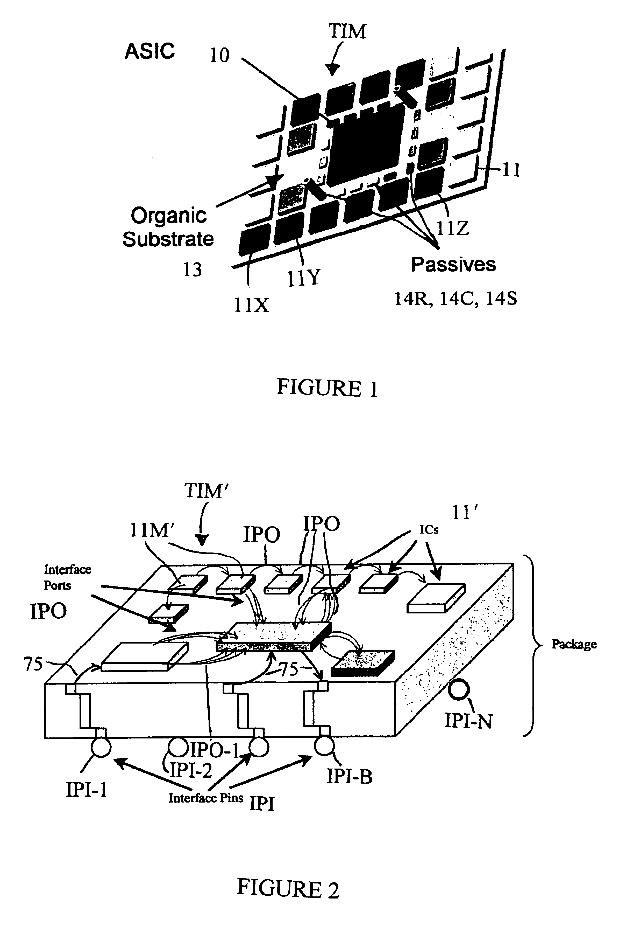
[0015]As discussed above, the tailored interconnect module device of the present invention seeks to reduce the number of interface pins coming to the module. Referring to FIG. 1, the tailored interconnect module (TIM) includes, for example, at its center, an application specific integrated circuit (ASIC) 10 which is surrounded by integrated circuit (IC) devices 11M, 11W, 11X, 11Y, 11Z, etc. which may be memory or functional devices in chip scale packages or bare die auxiliary devices. They are mounted on an organic substrate 13. Passive elements 14R, 14C, 14S, etc. such as resistors and capacitors, etc. may also be mounted on substrate 13.

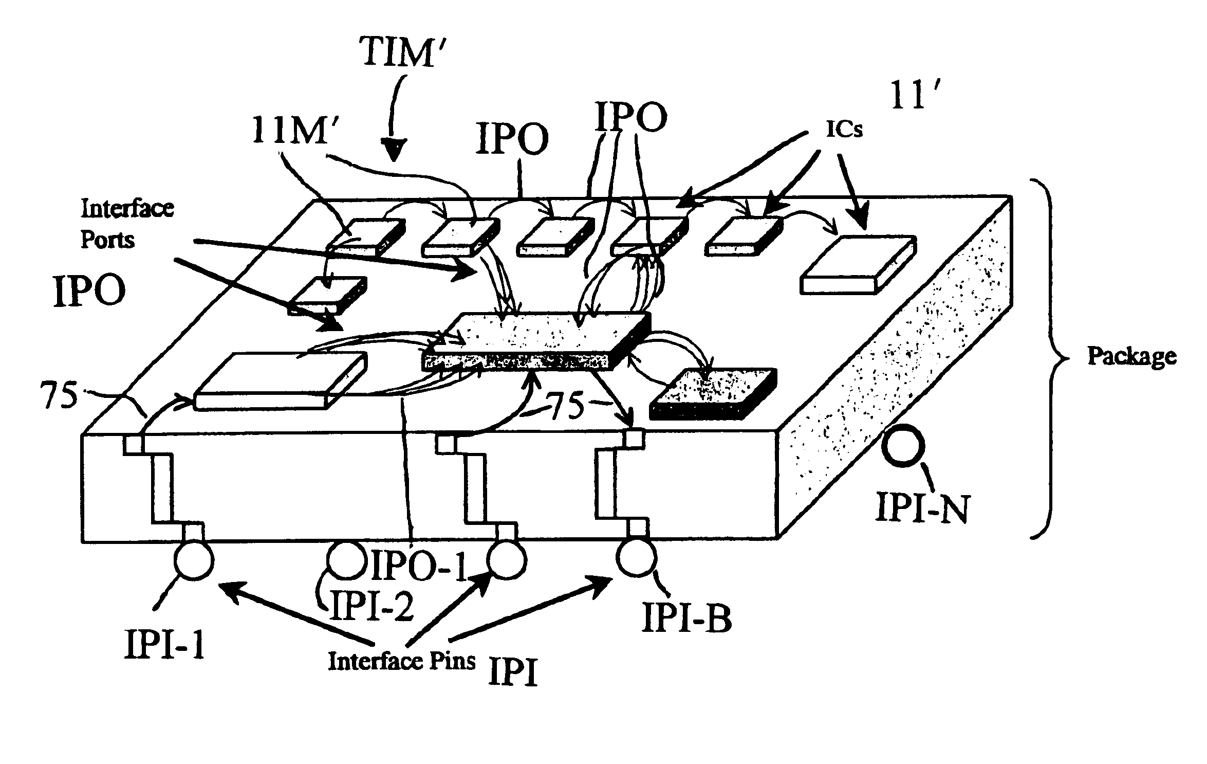
[0016]Referring now to FIG. 2, the ASIC 10′ is provided with connections for both interface ports IPO and interface pins IPI. In accordance with the practice of this invention, at least one bidirectional interface pin IPI-b is required as a minimum connection to the outside world for a useful tailored interconnect module according to the invention....


PUM


Abstract

An integrated circuit interconnect module for reducing interconnections between integrated circuit chips MOUNTED ON a support substrate. At least one primary integrated circuit (IC) device chip and a plurality of interacting peripheral integrated chip devices. The interconnect module including a plurality of interface pins, each integrated circuit device having a plurality of interface ports. At least one interface port of which is connected to another one of said plurality of integrated circuit devices, at least one of said integrated circuit devices having an interface port connected to an interface pin whereby the majority of nodes on the interacting peripheral devices are adapted to interface with nodes of the primary IC devices in such a way as to condense the number of nets so that the total number of nodes connected to external pins is minimized.

Description

BACKGROUND AND BRIEF DESCRIPTION OF THE INVENTION[0001]The invention is directed to the problem of alleviating routing constraints on boards having high pin count devices e.g. devices with a pin count in excess of 1000 pins.[0002]Current ASIC packaging uses a 1 mm spacing (pitch) between pins, which allows maximum package pin counts to be in the order of 2000 pins. Next generation packaging technology is expected to reduce this pitch to 0.8 mm in 2003 and to 0.65 mm by 2005. These pitches will enable packages of 2500 and 3000 pin counts to be implemented, respectively. However, as pin counts increase with decreasing pitch, routing circuit board connections (traces) to the pins becomes more difficult. This is because the pins are arranged in a grid, and with 0.65 mm to 1 mm spacing between pins, there is room enough to route only a single trace between pins. Consequently, multiple layer (or multi-layer) circuit boards are used, wherein each layer provides routing access to a row or t...

Claims


Application Information

Patent Timeline
Patent Type & Authority Patents(United States)
IPC IPC(8): H01L25/10H01L23/28H01L23/31H01L23/12
CPCH01L25/0655H01L25/16H01L23/3114H01L2924/1433H01L2924/3011H01L2924/0002H01L2924/00H01L2924/14H01L2924/1434H01L2924/15192H01L2924/15311H01L2924/19105H01L23/12
Inventor BROWN, PAUL
Owner ALCATEL LUCENT SAS
Why Eureka
Try Eureka