
Device and method for determining the lateral undercut of a structured surface layer

a structured surface layer and undercut technology, applied in semiconductor/solid-state device testing/measurement, electrical equipment, inductance, etc., can solve the problems of inadvertent etching too briefly or too long, and the permanent danger of destroying the structure on the wafer

Inactive Publication Date: 2005-06-28
ROBERT BOSCH GMBH
View PDF7 Cites 7 Cited by
  • Summary
  • Abstract
  • Description
  • Claims
  • Application Information

AI Technical Summary

Benefits of technology

[0003]An object of the present invention, therefore, was to make available a method and a device suitable for carrying it out, which make it possible, in an ongoing way, to measure the achieved undercut width and the extent of the undercut of a structured surface layer, during the undercutting process.
[0004]In contrast to the related art, the method according to the present invention, along with the device according to the present invention, has the advantage that it makes it possible to determine the extent of the lateral undercut of a structured surface layer by etching a sacrificial layer, in an ongoing manner, in situ, i.e., during the undercutting, as a function of time, and therefore to be able to monitor and adjust the undercut.
[0007]In this context, the transmitter and receiver, in a very advantageous manner, are located outside the actual etching chamber and thus remain protected from etching corrosion, in particular, from aggressive etching gases such as hydrofluoride acid vapor, ClF3, XeF2, and the like. Thus, in a way that is also very advantageous, it is possible to do without a costly interconnecting and contacting of the passive electronic component. The interaction of the passive component and the transmitter or receiver thus takes place, advantageously, without contact.
[0008]Furthermore, it is particularly advantageous if the transmitter and receiver are integrated in one assembly, in particular a processing unit and / or the transmitter is also a receiver. In particular, in the latter case, characteristic electrical parameters of the transmitter, which react to changes in an electromagnetic radiation field, such as internal voltages, currents, or phases between internal voltages and currents, can very expediently be detected or evaluated in a simple manner.
[0010]Similarly, it is advantageous if the second signal is also an electrical voltage, an absorbed or emitted intensity of an electromagnetic emission, an absorbed or emitted frequency, in particular, a resonance frequency, or a frequency spectrum of an electromagnetic emission.

Problems solved by technology

Therefore, the permanent danger exists of inadvertently etching too briefly or too long.
In particular, an etching lasting too long can lead to the destruction of structures on a wafer, for example, by detaching them from the substrate.

Method used


Image

  • Device and method for determining the lateral undercut of a structured surface layer
  • Device and method for determining the lateral undercut of a structured surface layer
  • Device and method for determining the lateral undercut of a structured surface layer

Examples


Embodiment Construction

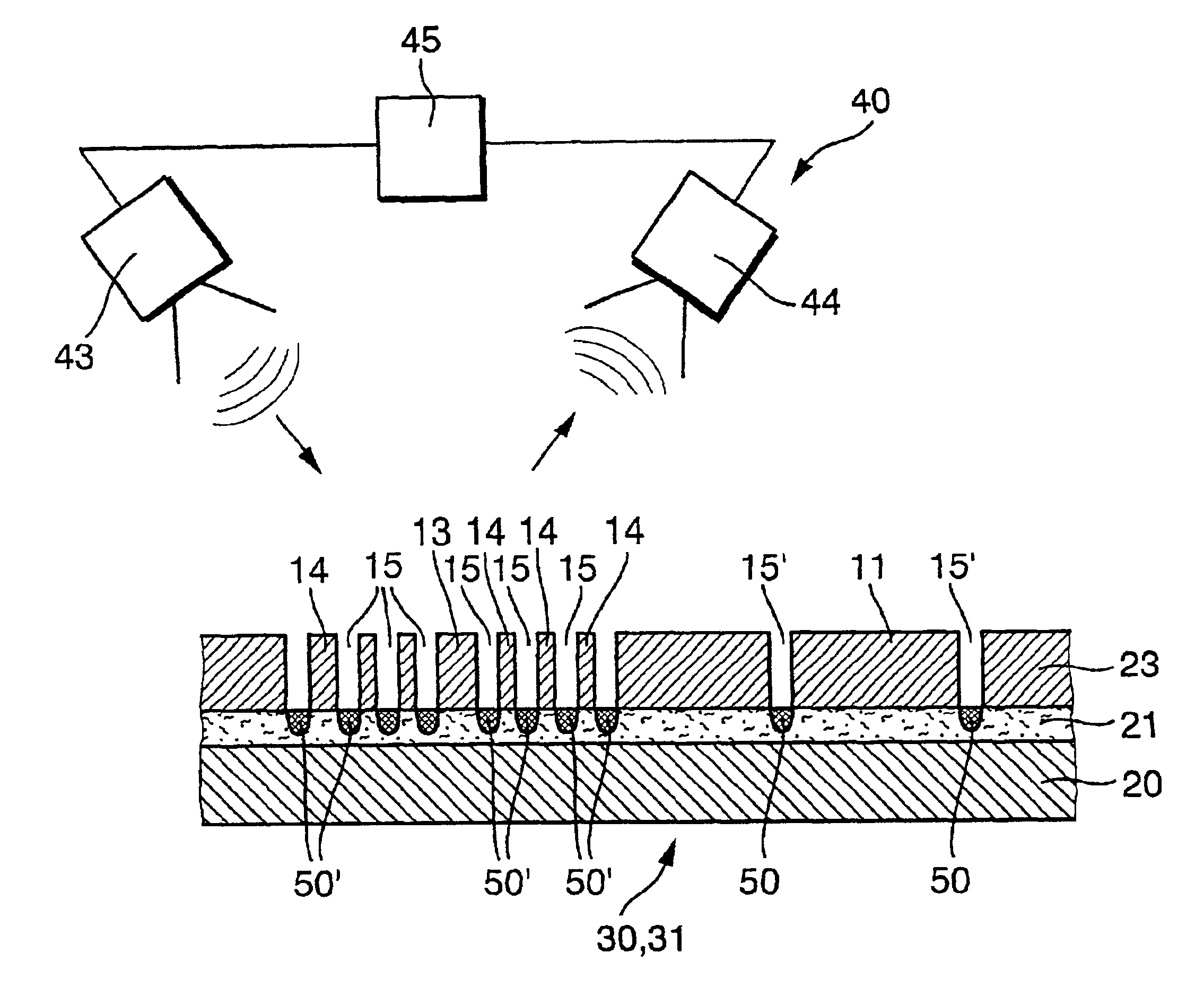
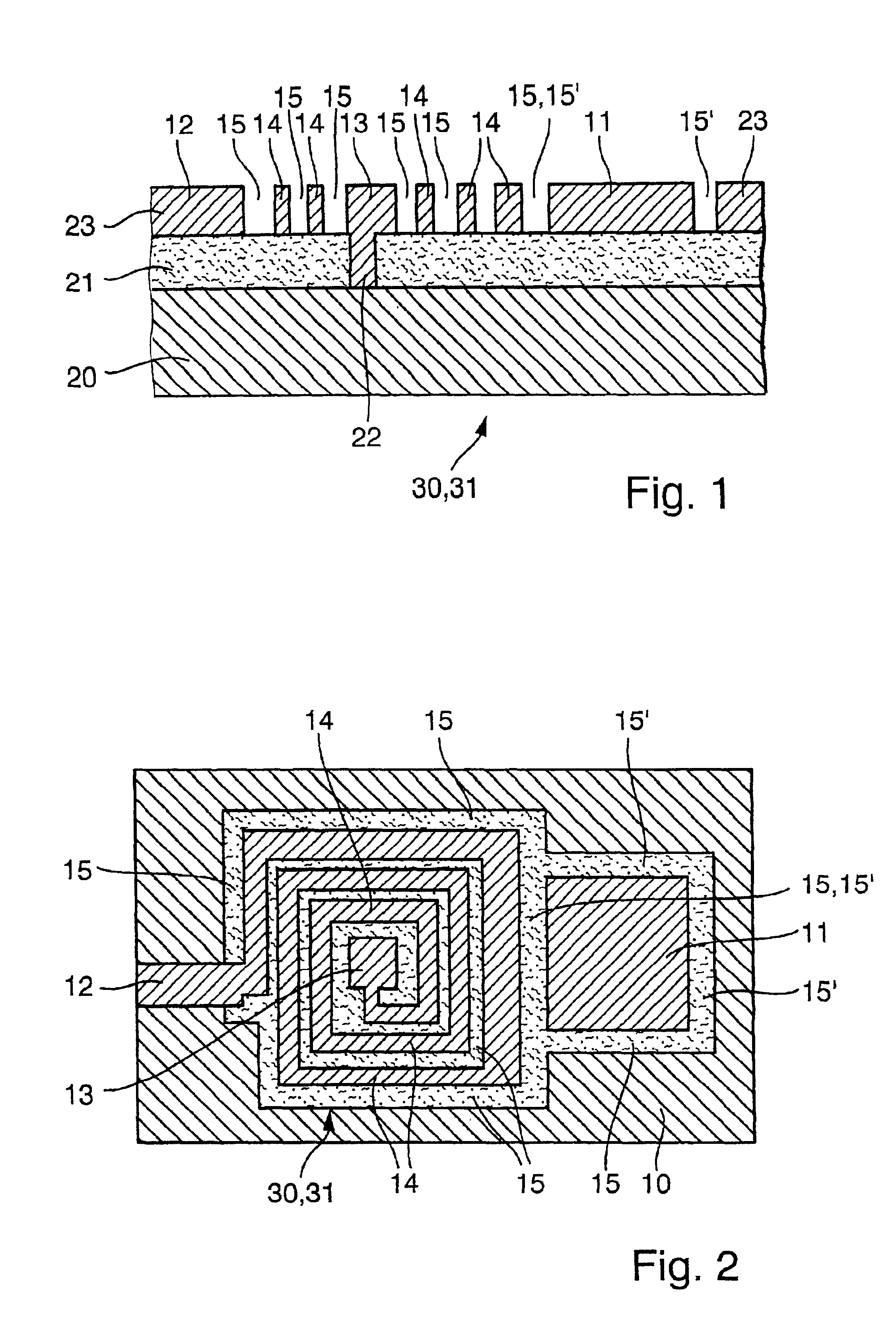
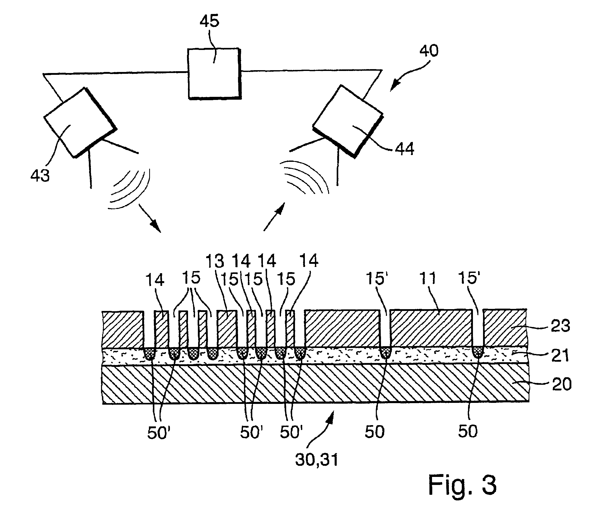
[0017]FIG. 1 depicts a layer arrangement having a structured surface layer 23, a sacrificial layer 21, and a base layer 20. Surface layer 23 is made of silicon or polysilicon, which is metallized on the surface, sacrificial layer 21 being made of silicon oxide, and base layer 20 being constituted by a silicon wafer. A design of this type has already been described, for example, in the German Published Patent Application 198 47 455. Furthermore, at least one passive electronic component 31 is locally delineated out from surface layer 23 in the form of a coil 30, coil 30 having a first coil end 13 and a second coil end 12 as well as coil windings 14, which are separated from each other via trenches 15, delineated out in surface layer 23 and extending in depth down to sacrificial layer 21. First coil end 13 is connected to base layer 20 via a plated through-hole 22, base layer 20 being electrically conductive. Coil 30 having inductance L thus constitutes, along with base layer 20, a ca...


PUM


Abstract

A device and a method for determining the extent of an at least locally lateral undercut of a structured surface layer on a sacrificial layer. The structured surface layer for this purpose locally has at least one passive electronic component, using which a physical measured quantity can be determined, which is proportional to the extent of the lateral undercut. The method for generating this device proposes, initially on the structured surface layer in a first etching method, to provide the surface layer at least locally with a structuring having trenches and, in a second etching method, proceeding from the trenches, to undertake at least locally a lateral undercut of the structured surface layer. In this context, in the first etching method on the surface layer, locally at least one passive electronic component is additionally delineated out, which in response to a subsequent undercutting of the surface layer is also undercut. The physical measured quantity is determined without contact, preferably by sending an electromagnetic emission into the passive component.

Description

FIELD OF THE INVENTION[0001]The present invention relates to a device and a method for determining an at least local lateral undercut of a structured surface layer.BACKGROUND INFORMATION[0002]It is known to etch micromechanical surface structures in a silicon layer in hydrofluoride acid vapor and, to achieve an undercut of a structured surface layer of silicon, to apply a sacrificial layer of silicon dioxide under the surface layer to be structured. In this context, the hydrofluoride acid vapor, in etching the sacrificial layer, effects a purely time-controlled undercut of the structured surface layer, so that the specific undercut width achieved in the sacrificial layer, for example, to bring about the defined exposure of free-standing sensor structures in the surface layer, is not directly measurable in the course of the hydrofluoride acid vapor undercut, or cannot be monitored during the etching. Therefore, the permanent danger exists of inadvertently etching too briefly or too l...

Claims


Application Information

Patent Timeline
Patent Type & Authority Patents(United States)
IPC IPC(8): H01L21/02H01L21/66B81C99/00
CPCB81C99/004H01L28/10H01L22/12H01L22/00
Inventor BECKER, VOLKERLAERMER, FRANZSCHILP, ANDREA
Owner ROBERT BOSCH GMBH
Learn More