Tape carrier semiconductor device

a semiconductor device and tape carrier technology, applied in the field can solve the problems of increasing the cost of tape carrier semiconductor devices in proportion to the tape area, forming a waste of manufacturing cost on the tape carrier, and wasting such areas, so as to save the manufacturing cost of tape carrier semiconductor devices

Inactive Publication Date: 2005-06-28
SHARP KK
View PDF28 Cites 29 Cited by
  • Summary
  • Abstract
  • Description
  • Claims
  • Application Information

AI Technical Summary

Benefits of technology

[0010]It is therefore an object of the present invention to save the manufacturing cost of the tape carrier semiconductor devices by increasing the number of devices manufactured out of a tape carrier of a certain length without losing the benefits that they can be designed in arbitrary shapes.

Problems solved by technology

However, when the tape carrier semiconductor devices of arbitrary shapes are aligned in a single direction, as has been discussed, a useless area which is not used in manufacturing the tape carrier semiconductor devices is formed on the tape carrier.
When the manufacturing procedure and used materials of the tape carrier are concerned, the tape carrier is manufactured in the form of a lengthy tape from reel to reel, and therefore, the cost thereof increases in proportion to the tape area.
Thus, even if some areas of the tape carrier are not used in manufacturing the tape carrier semiconductor devices, the cost wasted on such areas is included in the manufacturing cost.
Therefore, the manufacturing cost of the tape carrier semiconductor devices increases as the areas which are not used in manufacturing increases.
However, this is not preferable, because the design flexibility given to the tape carrier semiconductor devices as benefits will be lost.
However, the above publication does not solve the problem that useless areas are readily formed on the tape area if the tape carrier semiconductor devices are of arbitrary shapes, because each TAB is aligned in one specific direction with respect to a direction in which the tape is fed, and each TAB is of a rectangular shape with which the tape area can be utilized efficiently.

Method used


Image

  • Tape carrier semiconductor device
  • Tape carrier semiconductor device
  • Tape carrier semiconductor device

Examples


embodiment 1

(Embodiment 1)

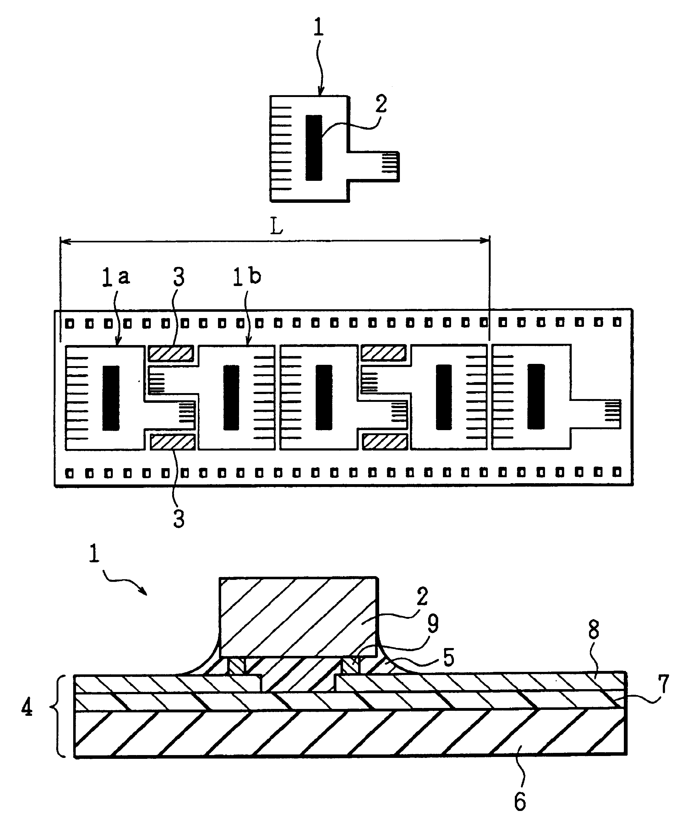
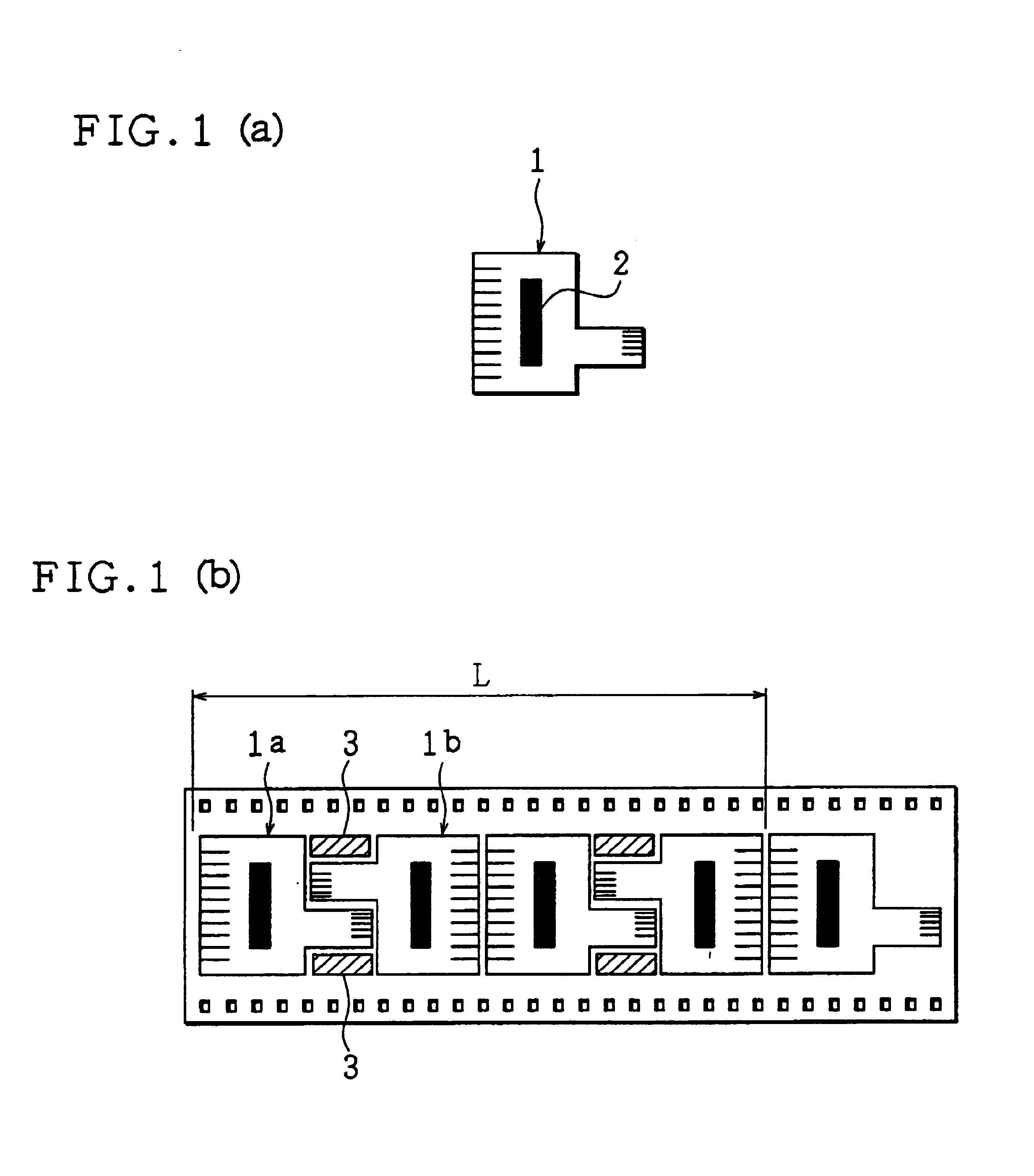
[0046]FIGS. 1(a) and 1(b) show the shape of the COF of the present embodiment and the layout of the COF patterns on the tape carrier, respectively.

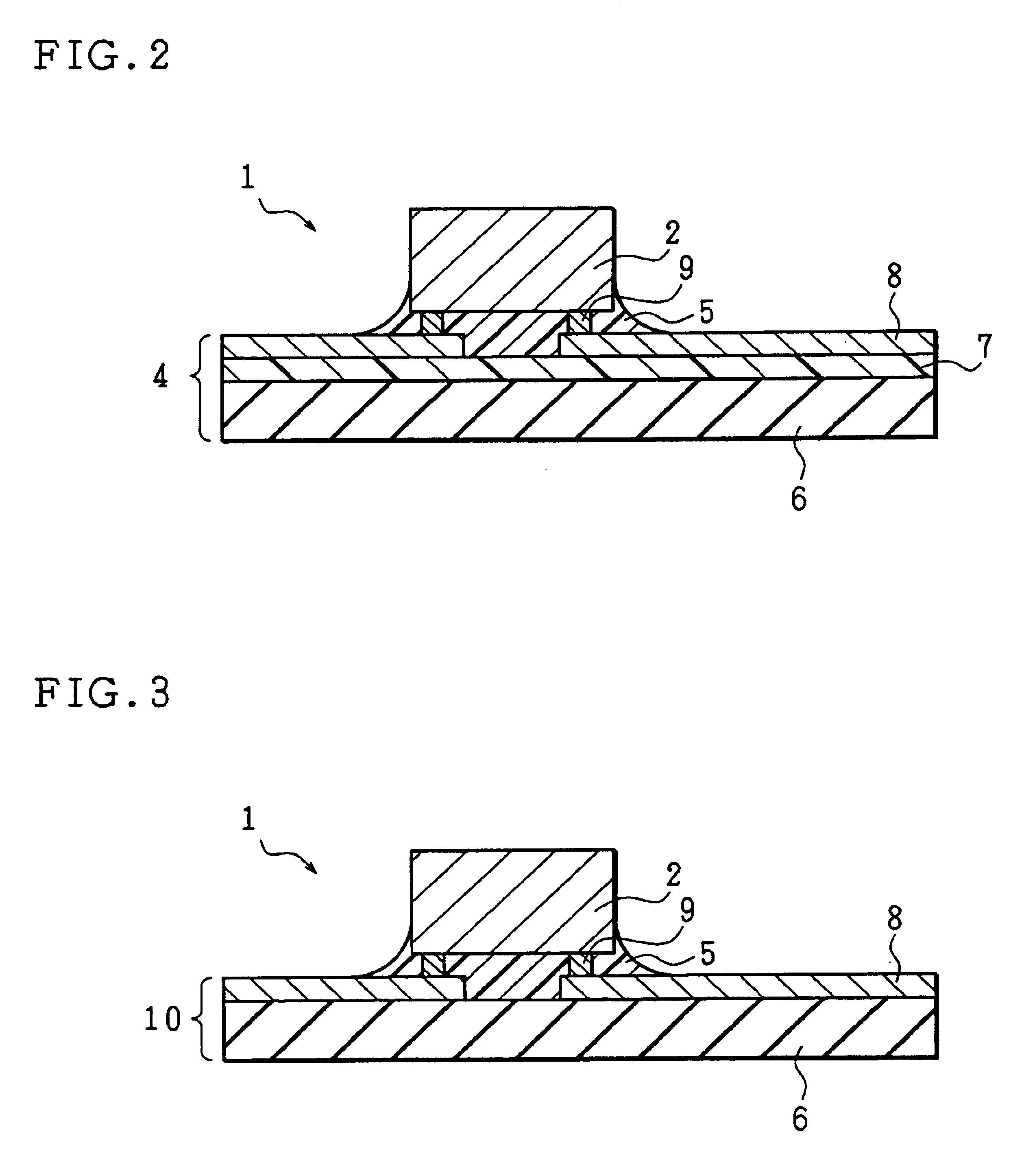
[0047]A COF 1 is of the shape shown in FIG. 1(a), which is identical with the shape of the COF 51 shown in FIG. 11 (a). The COF 1 is composed of a flexible printed board on which a wiring pattern has been formed, and a semiconductor element (indicated by black-paint) 2 bonded and mounted thereon. The wiring pattern is generally composed of an inner lead connected to the electrode of the semiconductor element 2 and an outer lead connected to an external circuit. In FIG. 1(a), the inner lead is omitted for ease of explanation.

[0048]In case that the COFs 1 are designed in a layout so as to be aligned on the tape carrier in accordance with the method of the present embodiment, adjacent COF patterns 1a and 1b are positioned on the tape carrier in such a manner that one is turned by 180 degrees with respect to the other. When punc...

embodiment 2

(Embodiment 2)

[0067]FIGS. 7(a) through 7(c) show another embodiment of the present invention.

[0068]A COF 11 of the present embodiment is of the shape shown in FIG. 7(a), and used in the liquid crystal module. In the liquid crystal module, more than one COF is mounted at both ends of the liquid crystal panel, and in such a case, drivers each composed of mirror symmetrical COFs are mounted respectively at the top and bottom (right and left) of the liquid crystal panel. The arrangement of the present embodiment is particularly effective in manufacturing the mirror symmetrical COFs.

[0069]According to the arrangement of the present embodiment, as shown in FIG. 7(b), the COFs 11a which are of the same shape as that of the COF 11 of FIG. 7(a) and COFs 11b which are mirror symmetrical with respect to the COFs 11a are aligned alternately on the same tape carrier 4. The COFs 11b are positioned where the COFs 11a are reversed from left to right and turned by 90 degrees counter clockwise in the...

embodiment 3

(Embodiment 3)

[0077]FIG. 8 shows still another embodiment of the present invention.

[0078]In the present embodiment, two kinds of COFs 13 and 14 of different shapes are aligned alternately on the same tape carrier 4. The COFs 13 and 14 are not necessarily used for the same module, and they can be used for different purposes when punched out. The COFs 13 and 14 are combined in such a manner that the pattern area on the tape carrier 4 can be utilized most efficiently (that is, useless areas which are not used in manufacturing the COFs are minimized).

[0079]FIG. 8 shows a case where two kinds of COFs are formed on the same tape carrier 4, but three or more kinds of COFs may be formed on the same tape carrier 4. In such a case, a plurality of kinds of COFs are aligned in a specific order.

[0080]As has been discussed, according to the arrangement of the present embodiment, more than one kind of COFs each having a different shape are simultaneously formed on the same tape carrier. By making ...


PUM


Abstract

In a COF manufactured by bonding and mounting a semiconductor element onto a wiring pattern on a lengthy tape carrier, the wiring patterns are aligned in more than one direction with respect to a direction in which the tape carrier is fed. The wiring patterns have a layout that increases a utilized area of the tape carrier (in other words, such that reduces useless areas). Consequently, the number of the tape carrier semiconductor devices manufactured out of a tape carrier of a certain length can be increased thereby saving manufacturing costs.

Description

FIELD OF THE INVENTION[0001]The present invention relates to a tape carrier semiconductor device composed of a flexible printed board and a semiconductor element bonded and mounted thereon, and a method of manufacturing the same.BACKGROUND OF THE INVENTION[0002]In packing semiconductor elements into an electronic circuit, a TAB (Tape Automated Bonding) technique has been known, by which a tape carrier semiconductor device is obtained by bonding and mounting a semiconductor element on a flexible printed board (so called tape carrier)[0003]Tape carrier semiconductor devices obtained by the TAB technique include a COF (Chip On FPC (Flexible Printed Circuit)), a TCP (Tape Carrier Package), etc. In the COF, the tape carrier is bonded to the semiconductor element electrode and a wiring pattern on the bonded portion is backed with a tape carrier material. On the other hand, in the TCP the tape carrier material is bonded to the semiconductor element electrode and a through-hole is provided ...

Claims


Application Information

Patent Timeline
Patent Type & Authority Patents(United States)
IPC IPC(8): H01L21/60H01L21/02H01L23/498H01L23/48H05K3/00H05K1/11H01L25/00
CPCH01L23/4985H05K3/0052H01L24/29H01L24/83H01L24/97H01L2224/32225H01L2224/16225H01L2224/73204H01L2224/83192H01L2224/838H01L2924/01004H01L2924/01005H01L2924/01015H01L2924/01029H01L2924/01033H01L2924/0105H01L2924/01078H01L2924/01079H01L2924/01082H01L2924/0781H01L2924/19041H01L2924/19043H05K1/117H05K2203/1545H01L2924/01006H01L2924/014H01L2924/0132H01L2924/07802H01L2924/1579H01L2224/29111H01L2924/12041H01L2924/07811H01L2224/29298H01L2924/00014H01L2924/00H01L2224/0401H01L25/00
Inventor CHIKAWA, YASUNORI
Owner SHARP KK
Why Eureka
Try Eureka