Apparatus for functional and stress testing of exposed chip land grid array devices

a grid array device and test apparatus technology, applied in the direction of electrical testing, measurement devices, instruments, etc., can solve the problems of affecting the thermal control performance of the assembly, and affecting the test volume, so as to facilitate high-volume testing, accurately position the contact portion, and enhance the thermal interface performance

Inactive Publication Date: 2005-06-28
IBM CORP
View PDF2 Cites 26 Cited by
  • Summary
  • Abstract
  • Description
  • Claims
  • Application Information

AI Technical Summary

Benefits of technology

[0008]The present invention teaches an innovative chip test system and nest assembly. In a preferred embodiment, the nest assembly provides an automated means of rapidly installing (and removing) a TCA or other exposed chip Land Grid Array (LGA) devices onto a test board site to facilitate high-volume testing. Preferred embodiments of the present innovative nest assembly include a custom pogo pin socket to electrically connect the TCA LGA substrate to the test board by mechanically loading the TCA substrate into a test socket. Preferred embodiments also include means to geometrically center the load placed on the coldplate and chip for enhanced thermal interface performance, and means to accurately position the contact portion of the coldplate within the chip footprint while allowing unrestrained planar alignment between the coldplate and chip surfaces.

Problems solved by technology

Previous test apparatus suffered from shortcomings, such as the inability to accurately and repeatedly register the coldplate with respect to the TCA chip surface, which can contribute to chip damage.
Further, the external loads applied to the coldplate were not well balanced, resulting in a poorly centered contact load between the coldplate and chip surface, which detracts from the thermal control performance of the assembly.

Method used


Image

  • Apparatus for functional and stress testing of exposed chip land grid array devices
  • Apparatus for functional and stress testing of exposed chip land grid array devices
  • Apparatus for functional and stress testing of exposed chip land grid array devices

Examples


Embodiment Construction

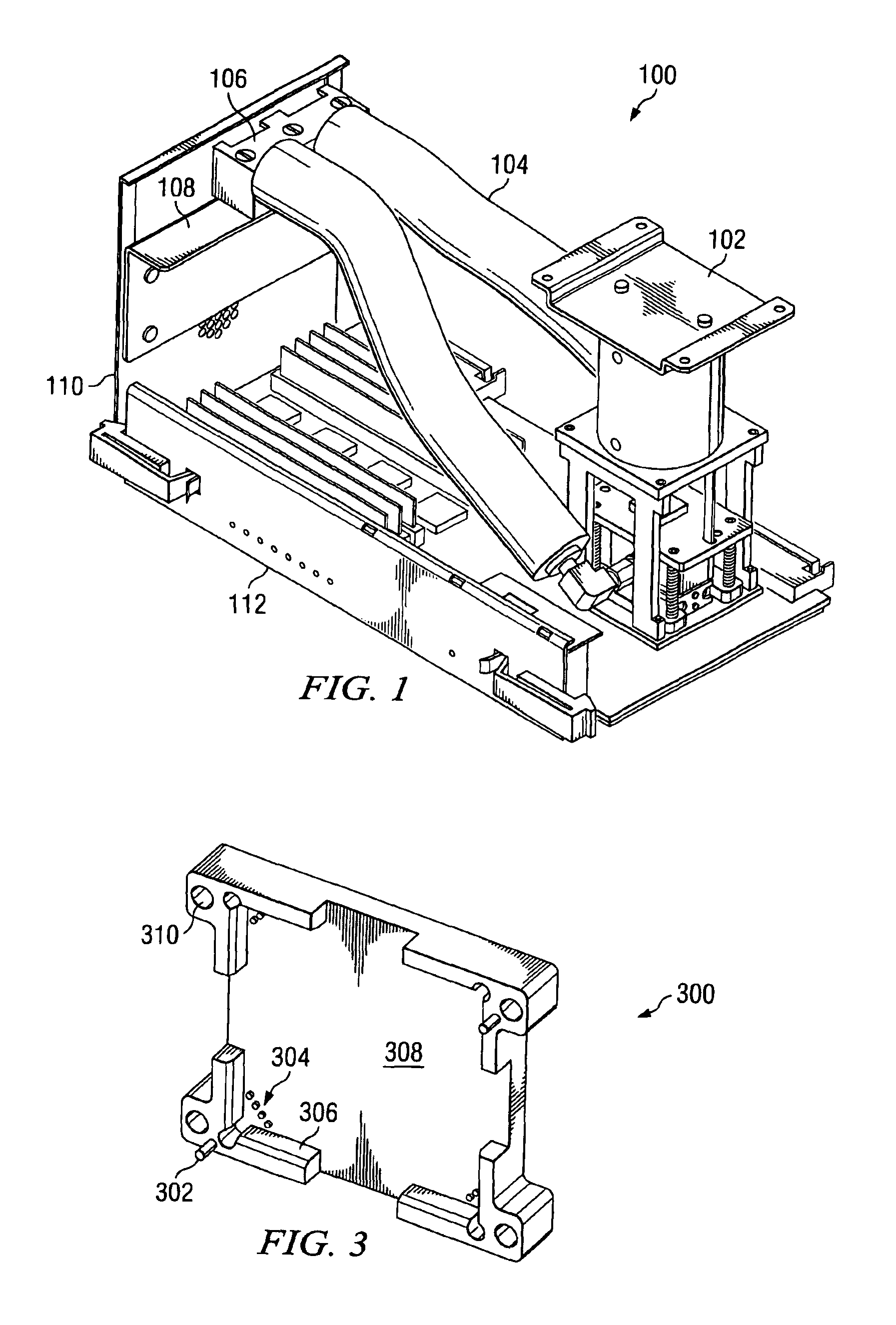
[0018]FIG. 1 shows an innovative nest and test card assembly consistent with a preferred embodiment. The nest is part of a chip testing system and includes the region and apparatus where the DUT is retained inside the testing system.

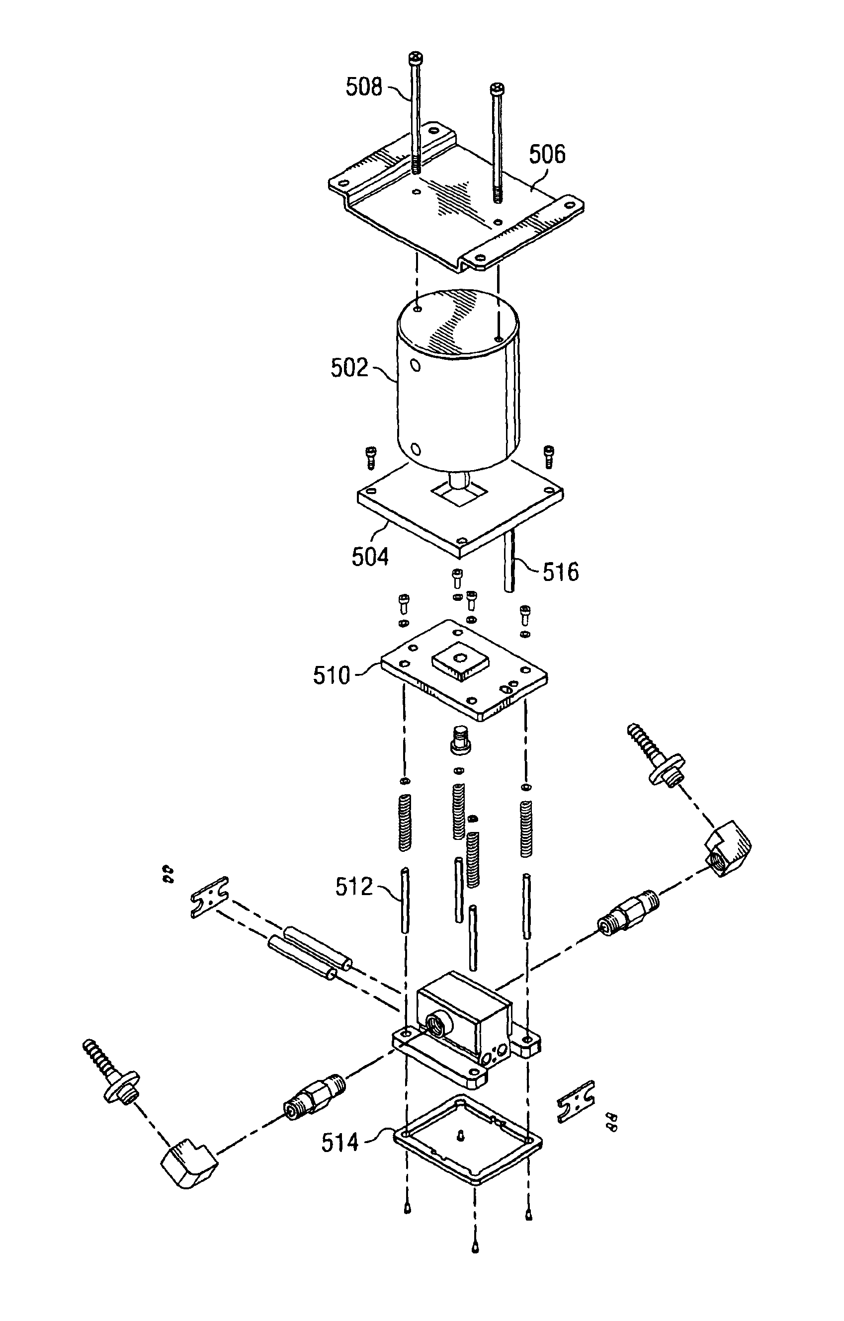
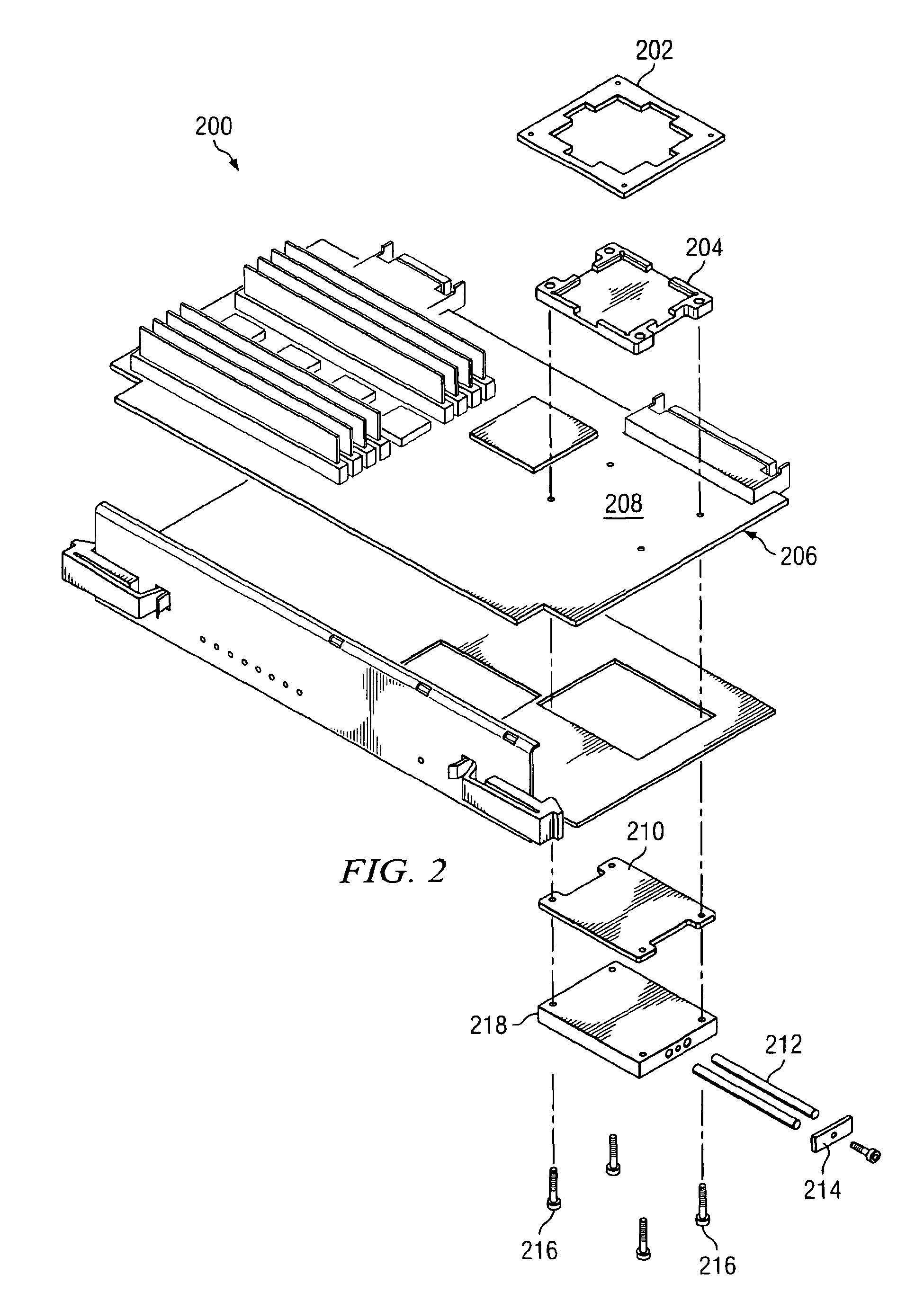
[0019]The primary components include air cylinder and coldplate assembly 102 which is mounted directly to test card book assembly 112. Test card book assembly 112 is installed in a card cage where it is connected to a tester backplane. The rear end of the card cage contains bulkhead 110. Coolant line clamp 106 is mounted to clamp support bracket 108, which is mounted to bulkhead 110. Insulated coolant lines 104 supply chilled fluid to the nest region (specifically the coldplate or heat sink) to control temperature of the DUT.

[0020]The thermal performance of the system, i.e., uniformity of cooling of the DUT by the coldplate, is sensitive to the net force driving the DUT and coldplate together. The contact between the two should be as uniform as possible,...


PUM


Abstract

A chip testing system with improved thermal performance. In a preferred embodiment, a nest assembly of a chip testing apparatus includes tooling balls and a fitted frame for improving alignment of a coldplate and a chip surface. In preferred embodiments, the coldplate is of unibody design. Thermal performance is also improved by balancing the forces exerted on the coldplate using an adjustable hose mounting bracket. The bracket allows the forces exerted by the hoses on the coldplate to be adjusted so they balance and cancel other unwanted forces on the cold plate.

Description

BACKGROUND OF THE INVENTION[0001]1. Technical Field[0002]The present invention relates generally to integrated circuit chip testing, and particularly to an improved functional and stress testing apparatus.[0003]2. Description of Related Art[0004]High performance processor chips are frequently sorted by various high performance metrics so they can be matched with the class of machine for which they are intended. This typically involves investigating chip performance using functional test sequences at the extremes of various operational windows for several variables, among these being chip voltage, clock speed, power, and temperature. These test sequences at temperature extremes can also identify early life failures and reduce the likelihood of a faulty chip escaping and being assembled into high-function and high-cost devices.[0005]Processor chips are typically attached to a temporary carrier (e.g., a temporary chip attach, or TCA) and then installed in a device tester. The tester co...

Claims


Application Information

Patent Timeline
Patent Type & Authority Patents(United States)
IPC IPC(8): G01R31/26
CPCG01R31/2891
Inventor CANNON, LONNIE J.CORBIN, JR., JOHN SAUNDERSGARDELL, DAVID LEWISGARZA, JOSE ARTUROKUTNER, JEFFREY FRANKLARSEN, KENNETH CARLMAHANEY, JR., HOWARD VICTORSALAZAR, JOHN JOSEPH
Owner IBM CORP
Why Eureka
Try Eureka