

Projection optical system, a projection exposure apparatus, and a projection exposure method
a technology of optical system and exposure apparatus, applied in the direction of photomechanical apparatus, instruments, printers, etc., can solve the problems of limited materials that can transmit radiated ultraviolet or vacuum ultraviolet beams, low transmissivity of such limited materials, and limited materials, etc., to achieve excellent image forming performance
- Summary
- Abstract
- Description
- Claims
- Application Information
AI Technical Summary
Benefits of technology
Problems solved by technology
Method used
Image

Examples
first embodiment
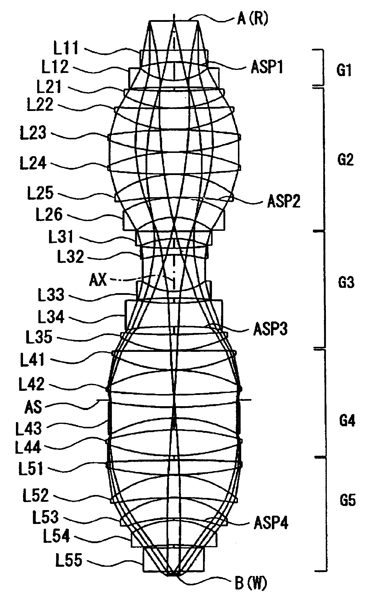
[0048]FIG. 1 is an optical path diagram of the projection optical system according to the The projection optical system of this embodiment uses 248.4 nm as a standard wavelength. All of the light transmissive refractive members (lenses L11-L55) in the projection optical system are formed of silica glass (synthetic silica).
[0049]As shown in FIG. 1, the projection optical system of the first embodiment has, in order from the first plane A, a first lens group G1 having a negative refractive power, a second lens group G2 having a positive refractive power, a third lens group G3 having a negative refractive power, a fourth lens group G4 having an aperture stop AS in the optical path, and a fifth lens group G5 having a positive refractive power. An clear aperture of a lens surface in the projection optical system, in a direction from the first plane A towards the second plane B, monotonically increases in the first lens group G1, tends to change from increasing to decreasing in the secon...
second embodiment
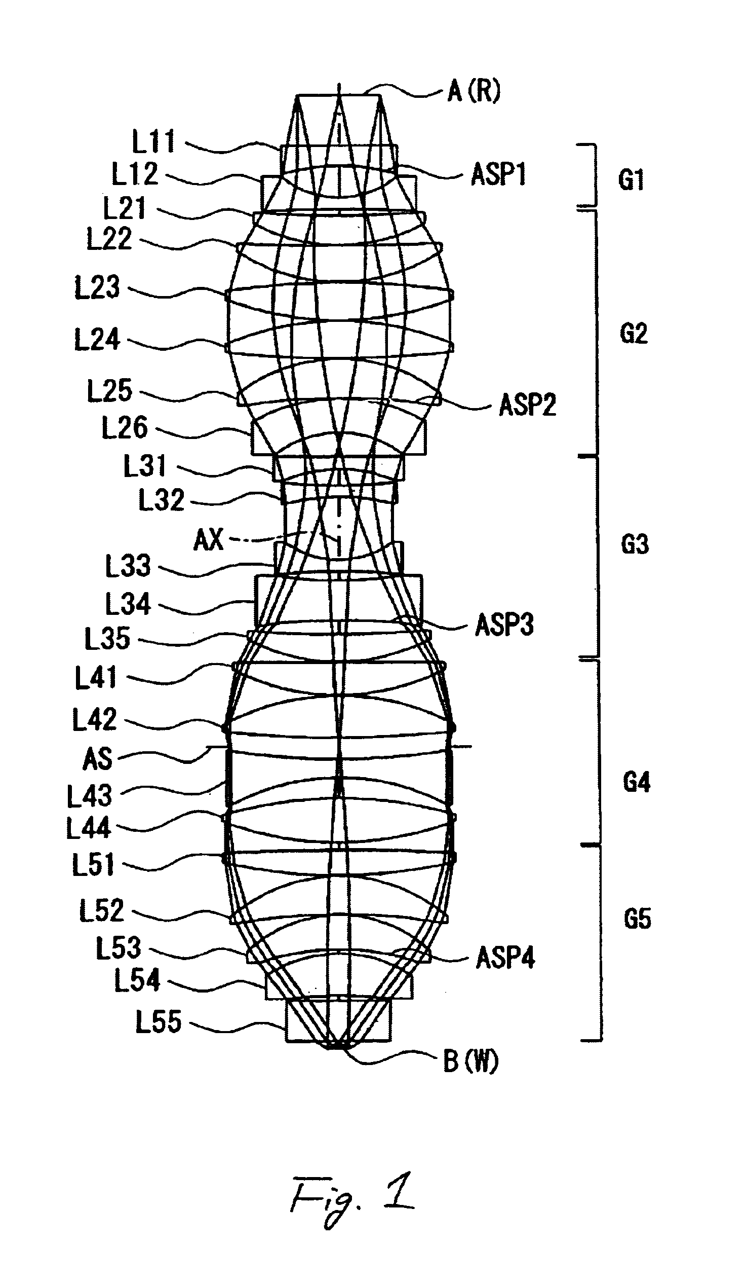
[0056]As shown in FIG. 2, the projection optical system of the second embodiment has, in order from the first plane A, a first lens group G1 having a negative refractive power, a second lens group G2 having a positive refractive power, a third lens group G3 having a negative refractive power, a fourth lens group G4 having an aperture stop AS in the optical path, and a fifth lens group G5 having a positive refractive power. An clear aperture of a lens surface in the projection optical system, in a direction from the first plane A towards the second plane B, monotonically increases in the first lens group G1, tends to change from increasing to decreasing in the second lens group G2, tends to change from decreasing to increasing in the third lens group G3, and monotonically decreases in the fifth lens group G5. In addition, the clear aperture of the lens surface in the projection optical system becomes a relative maximum in the second lens group G2, a relative minimum in the third lens...
third embodiment
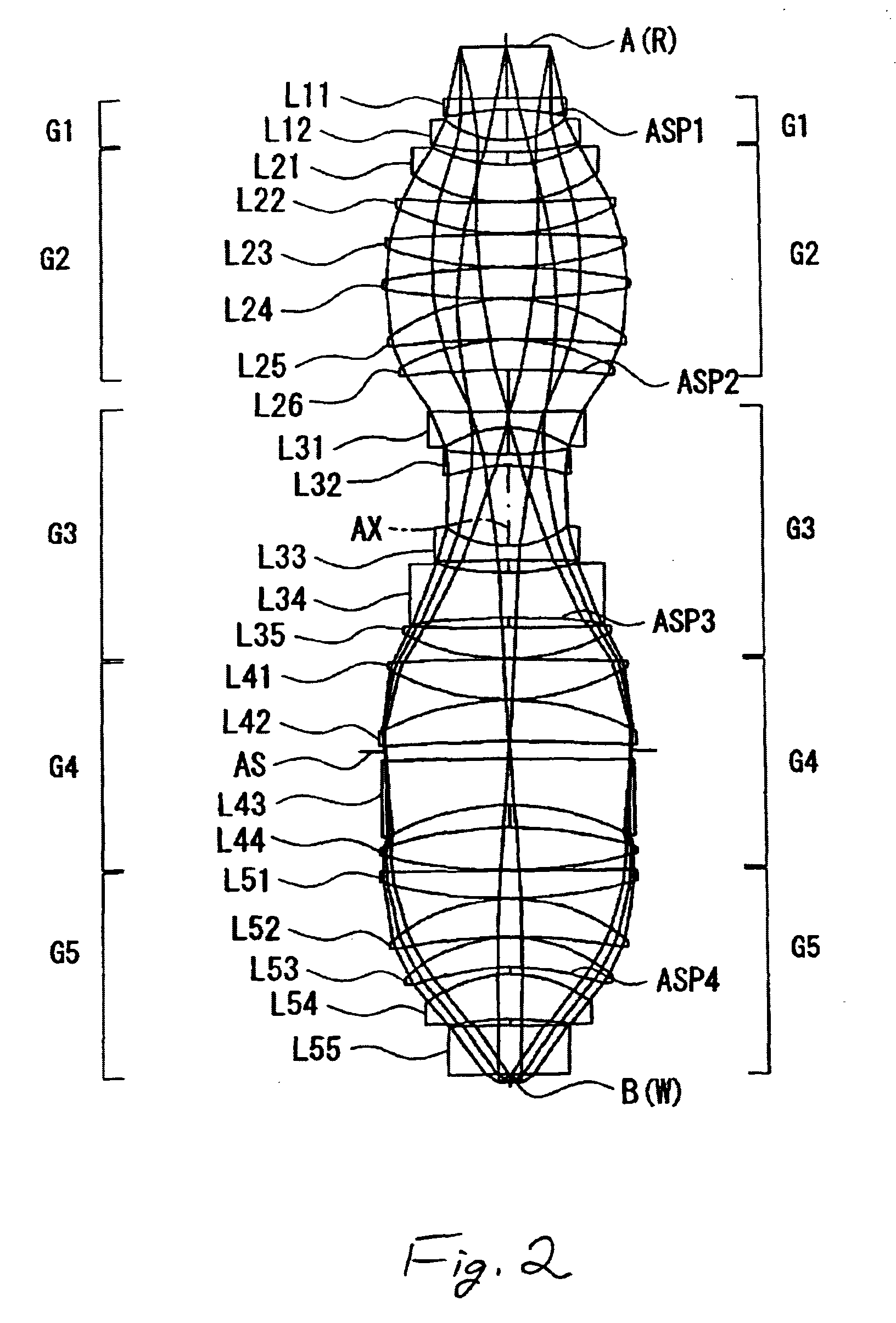
[0063]As shown in FIG. 3, the projection optical system of the third embodiment has, in order from the first plane A, a first lens group G1 having a negative refractive power, a second lens group G2 having a positive refractive power, a third lens group G3 having a negative refractive power, a fourth lens group G4 having an aperture stop AS in the optical path, and a fifth lens group G5 having a positive refractive power. An clear aperture of a lens surface in the projection optical system, in a direction from the first plane A toward the second plane B, monotonically increases in the first lens group G1, tends to change from increasing to decreasing in the second lens group G2, tends to change from decreasing to increasing in the third lens group G3, and monotonically decreases in the fifth lens group G5. In addition, the clear aperture of the lens surface in the projection optical system becomes a relative maximum in the second lens group G2, a relative minimum in the third lens g...
PUM
| Property | Measurement | Unit |
|---|---|---|
| wavelength | aaaaa | aaaaa |
| wavelength | aaaaa | aaaaa |
| wavelength | aaaaa | aaaaa |
Abstract
Description
Claims
Application Information