Shift register, display apparatus and information display apparatus
a technology of display apparatus and shift register, which is applied in the direction of static indicating devices, instruments, solid-state devices, etc., to achieve the effects of reducing the certainty of operation, increasing the number of wiring, and deteriorating the signal
- Summary
- Abstract
- Description
- Claims
- Application Information
AI Technical Summary
Benefits of technology
Problems solved by technology
Method used
Image

Examples
embodiment 1
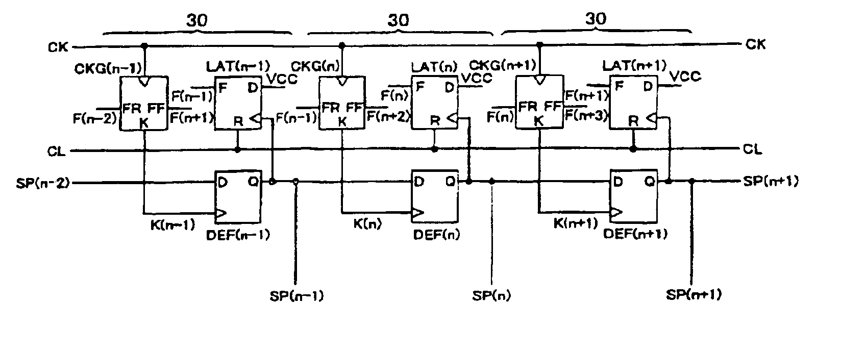
[0073]Firstly, this invention will be described by use of FIG. 1 showing an embodiment 1 which will be described later, but this invention is not limited to this embodiment.
[0074]As shown in FIG. 1, in this invention, provided are a plurality of shift pulse generation units 30 (hereinafter, simply referred to unit) each of which includes pulse generation portion (a register circuit DFF(n): n is an integer and the same is applied below), a status signal generation part (a latch circuit LAT(n) as the status signal generation circuit), and a clock extraction part (a clock gate circuit CKG(n)) which is a clock supply circuit.
[0075]A clock signal line (CK) through which clock signals are inputted to all units 30 is connected to each clock extraction part CKG.
[0076]With regard to the pulse generation portion DFF, in the same manner as in a conventional shift register, Q output terminals and D input terminals are connected in sequence between the pulse generation portions DFF so as to gene...
embodiment 2
[0155][Embodiment 2]
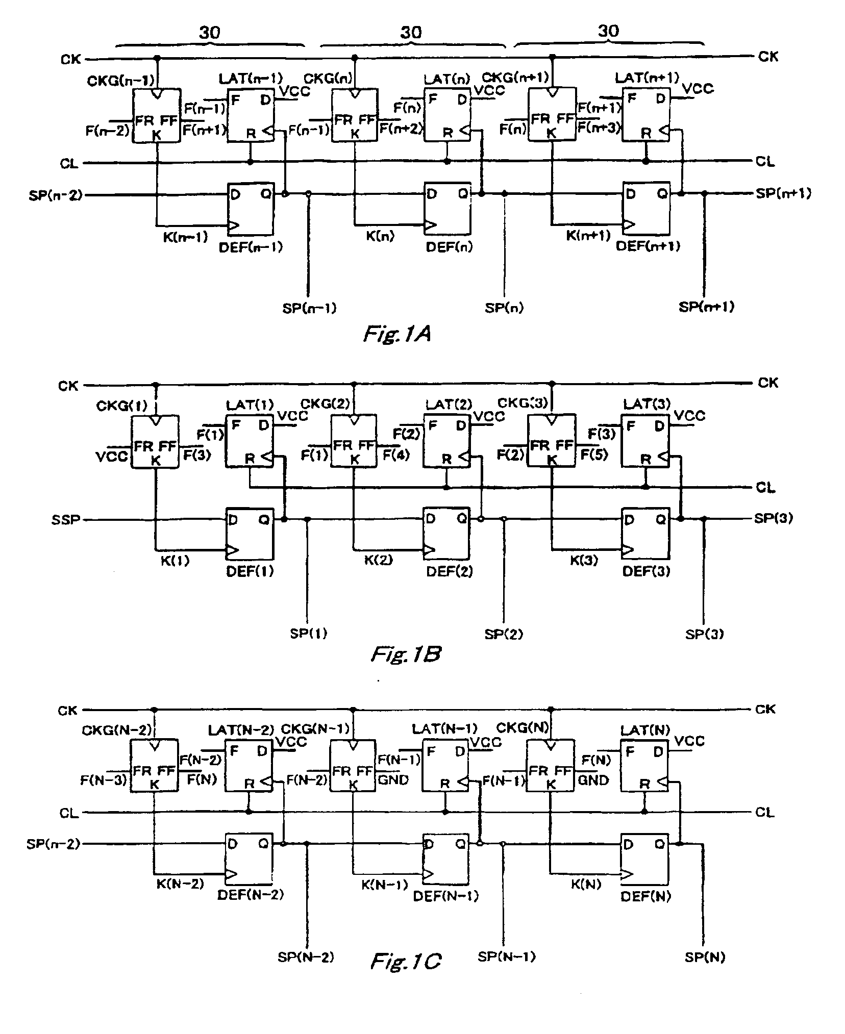
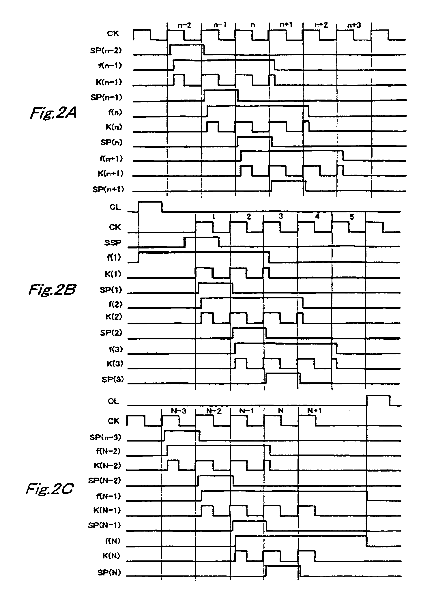
[0156]FIGS. 3A to 3C show another embodiment of a shift register of this invention, and in the same manner as in the conventional shift register of FIG. 8, it generates a group of 2N pieces of pulse signals. Unless otherwise noted, terminals, signals and the like with the same reference numerals and signs as in FIG. 1 represents ones which have the same operations and functions. In addition, in this embodiment, a pair of register circuits Da(n) and Db(n) correspond to the pulse generation portion, respectively.
[0157]
[0158]FIG. 3A shows three units 30 of (n−1)th, (n)th and (n+1)th which were arranged arbitrarily in between.
[0159]The input clock signal CK is inputted to respective clock signal input terminals of the clock gate circuits CKG(n−1), CKG(n) and CKG(n+1).
[0160]From the extraction clock output terminal K of CKG(n−1), the clock signal K(n−1) is outputted and inputted to the extraction clock signal input terminals of the register circuit Da(n−1) and Db(n−1)...
embodiment 3
[0211][Embodiment 3]
[0212]FIG. 7B shows a CKG circuit which can further reduce power consumption as compared to the CKG circuit of FIG. 7A which is used in the shift registers of the embodiments 1 and 2 which used this invention.
[0213]The clock signal input terminal CLK is inputted to an extraction switch which is configured by M9 and M10, and the other end of the extraction switch is connected to a reset switch which is configured by M11 between the other end of the switch and the ground GND, and inputted to a clock buffer circuit (clock output part) which comprises M12 to M15, and the positive clock ck and the negative clock nck are outputted.
[0214]Also, to M10 / G, the positive clock gate signal f is connected, and to M9 / G and M11 / G, the negative clock gate signal Nf is connected. Since channel capacity Cox of a MOS transistor does not function as capacity when a channel is shut off, there remains only coupling capacitance which is smaller than the channel capacity Cox between a ga...
PUM
 Abstract
Description
Claims
Application Information
 - R&D
- Intellectual Property
- Life Sciences
- Materials
- Tech Scout
- Unparalleled Data Quality
- Higher Quality Content
- 60% Fewer Hallucinations
Browse by: Latest US Patents, China's latest patents, Technical Efficacy Thesaurus, Application Domain, Technology Topic, Popular Technical Reports.
© 2025 PatSnap. All rights reserved.Legal|Privacy policy|Modern Slavery Act Transparency Statement|Sitemap|About US| Contact US: help@patsnap.com