Method for producing a multi-chip circuit module including a multi-layered wiring section utilizing a via-on-via structure

Inactive Publication Date: 2005-07-19
SONY CORP
View PDF9 Cites 51 Cited by
  • Summary
  • Abstract
  • Description
  • Claims
  • Application Information

AI Technical Summary

Benefits of technology

[0008]It is therefore an object of the present invention to provide a multi-chip circuit module, whereby the prob

Problems solved by technology

In the multi-chip circuit module, even if the clock frequencies exceeding the GHz order is achieved within each device (chip), the

Method used


Image

  • Method for producing a multi-chip circuit module including a multi-layered wiring section utilizing a via-on-via structure
  • Method for producing a multi-chip circuit module including a multi-layered wiring section utilizing a via-on-via structure
  • Method for producing a multi-chip circuit module including a multi-layered wiring section utilizing a via-on-via structure

Examples


Embodiment Construction

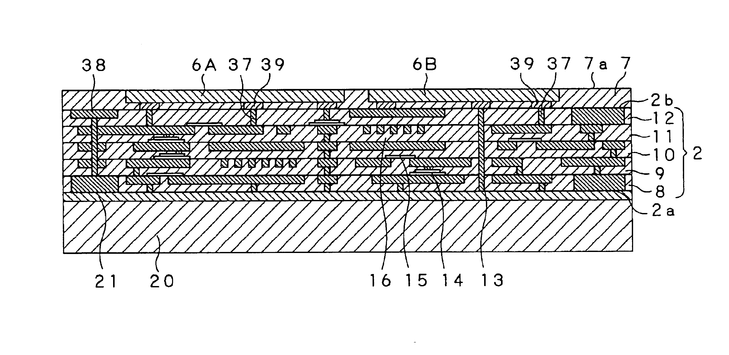
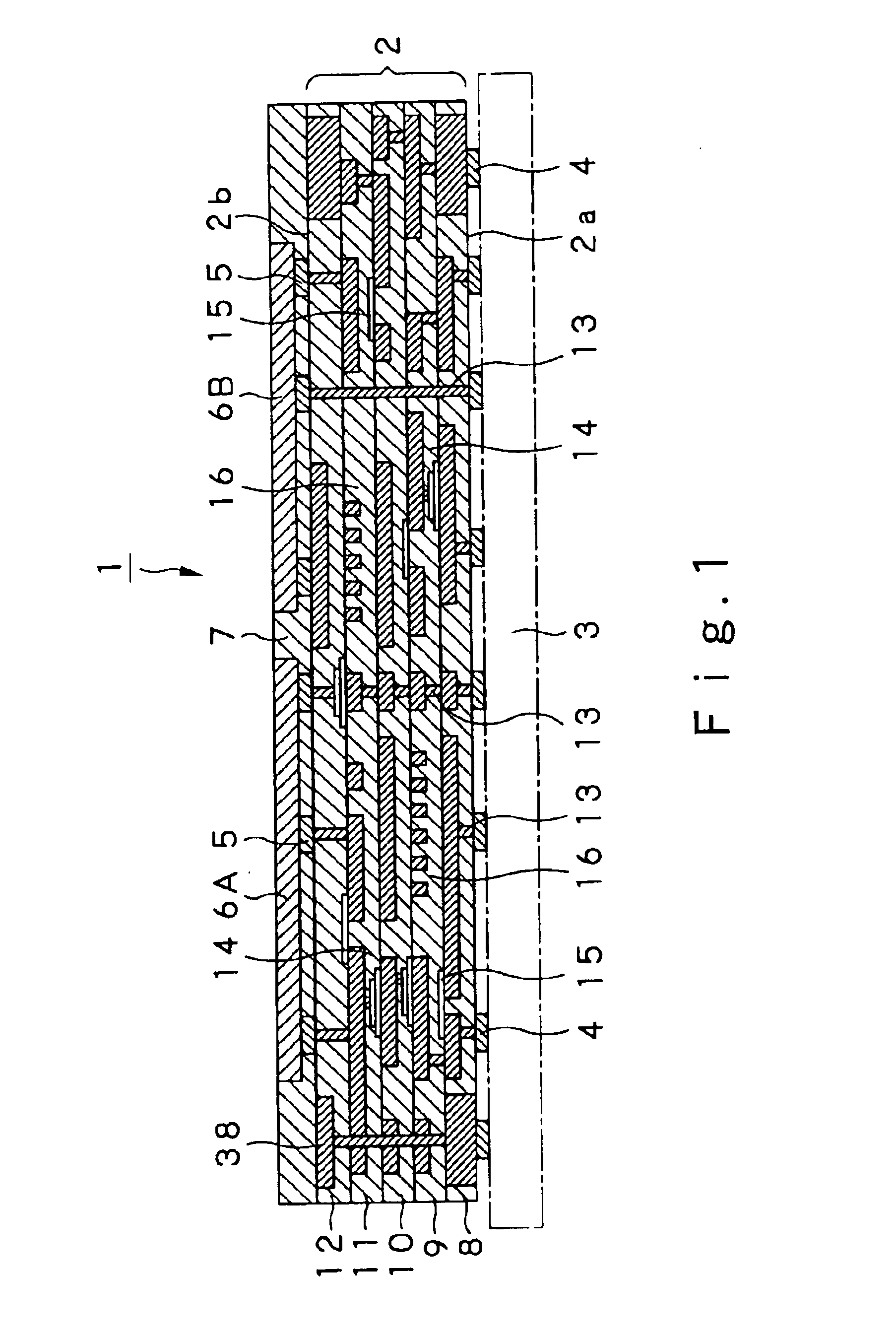
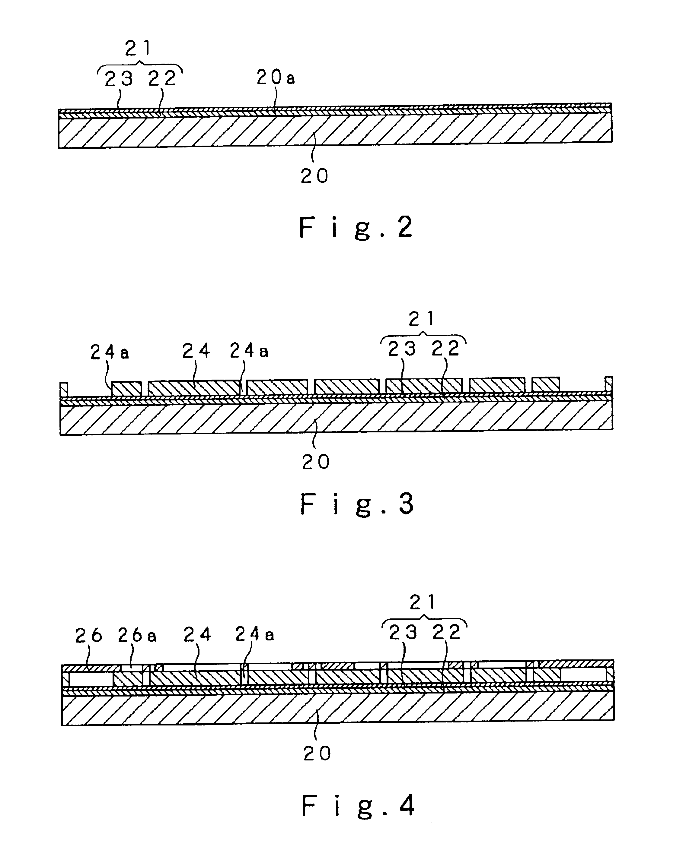
[0055]Referring to the drawings, certain preferred embodiments of the present invention are explained in detail.

[0056]A multi-chip circuit module 1, referred to below simply as a circuit module 1, embodying the present invention, has e.g., an information communication function or a storage function, and forms a high frequency circuit of an ultra-small-sized communication functional module unit, which is loaded on a variety of electronic equipment, such as a portable telephone set or an audio equipment, or which is inserted or unloaded as an optional device. Although not shown in detail, the circuit module 1 includes a high frequency transmitting / receiving circuit section by a superheterodyne system of converting the transmitted / received signal to an intermediate frequency or a high frequency transmitting / receiving circuit section by a direct conversion system of transmitting / receiving information signals without conversion to an intermediate frequency.

[0057]Referring to FIG. 1, the ...


PUM


Abstract

A multi-chip circuit module on which semiconductor chips are loaded and which is provided with circuit patterns, input/output terminals or the like for interconnecting the semiconductor chips. A multi-layered wiring section (2) is formed by respective unit wiring layers (8) to (12) in such a manner that an upper unit wiring layer is layered on a surface-planarized subjacent unit wiring layer and connected to one another by inter-layer connection by a via-on-via structure. A semiconductor chip (6) mounted on this multi-layer wiring section (2) is polished along with the sealing resin layer (7) for reducing the thickness.

Description

TECHNICAL FIELD[0001]This invention relates to a multi-chip circuit module, having a plurality of semiconductor chips, such as ICs or LSIs, loaded thereon, and also having circuit patterns, interconnecting the semiconductor chips, and input / output terminals, formed thereon, and a manufacturing method for the multi-chip circuit module. This application claims priority of Japanese Patent Application No. 2001-358246, filed on Nov. 22, 2001, the entirety of which is incorporated by reference herein.BACKGROUND ART[0002]A multi-chip circuit module, having a plurality of semiconductor chips, such as ICs or LSIs, loaded thereon, is provided to electronic equipment adapted for handling digital signals, such as personal computers, portable telephone sets, video equipment or audio equipment. In this sort of the electronic equipment, attempts are made to reduce the size, weight and the thickness as well as to improve the performance and functions, diversify the functions and to expedite the pro...

Claims


Application Information

Patent Timeline
IPC IPC(8): H01L25/065H01L23/52H01L23/28H01L23/31H01L21/68H01L23/538H01L21/98H01L21/67H01L21/70H01L25/10H05K3/46H01L21/56H01L21/02H05K3/00H01L25/04H01L25/18H01L29/00
CPCH01L23/3121H01L23/5385H01L23/5389H01L25/0652H01L25/0655H01L25/105H01L25/50H05K3/4647H05K3/4682H01L21/6835H01L21/563H01L2224/16235H01L2221/68345H01L2221/68359H01L2221/68363H01L2224/16225H01L2224/48091H01L2224/73204H01L2224/73253H01L2924/01004H01L2924/01078H01L2924/01079H01L2924/15311H01L2924/19041H01L2924/19107H01L2924/30105H01L2924/30107H01L2924/3011H05K3/007H05K2203/016H01L2224/81005H01L2924/10253H01L2225/1058H01L24/48H01L2924/01322H01L2924/18161H01L2924/3511H01L2225/1023H01L2924/00014H01L2924/00H01L2924/12042H01L2924/181H01L2224/05599H01L2224/45099H01L2224/85399H01L2924/14H01L2224/73257H01L2924/00012H01L2224/45015H01L2924/207H01L23/12
Inventor OGAWA, TSUYOSHINISHITANI, YUJI
Owner SONY CORP
Why Eureka
Try Eureka