Semiconductor device incorporating a defect controlled strained channel structure and method of making the same

a technology of defect control and straining channel structure, which is applied in the direction of semiconductor devices, basic electric elements, electrical equipment, etc., can solve the problems of not being able to controllable enough for manufacturing and difficult fabrication of sloped sidewall isolation structur

Inactive Publication Date: 2005-07-19
MOTOROLA INC +1
View PDF32 Cites 107 Cited by
  • Summary
  • Abstract
  • Description
  • Claims
  • Application Information

AI Technical Summary

Problems solved by technology

In addition, fabrication of a sloped sidewall isolation structure is difficult with current process tools and may not be controllable enough for manufacturing.

Method used


Image

  • Semiconductor device incorporating a defect controlled strained channel structure and method of making the same
  • Semiconductor device incorporating a defect controlled strained channel structure and method of making the same
  • Semiconductor device incorporating a defect controlled strained channel structure and method of making the same

Examples


Embodiment Construction

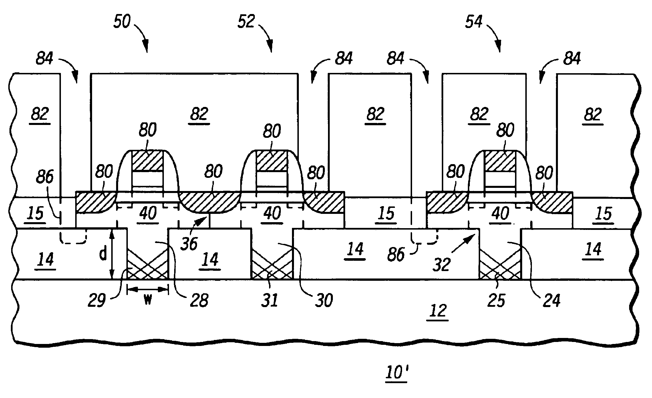
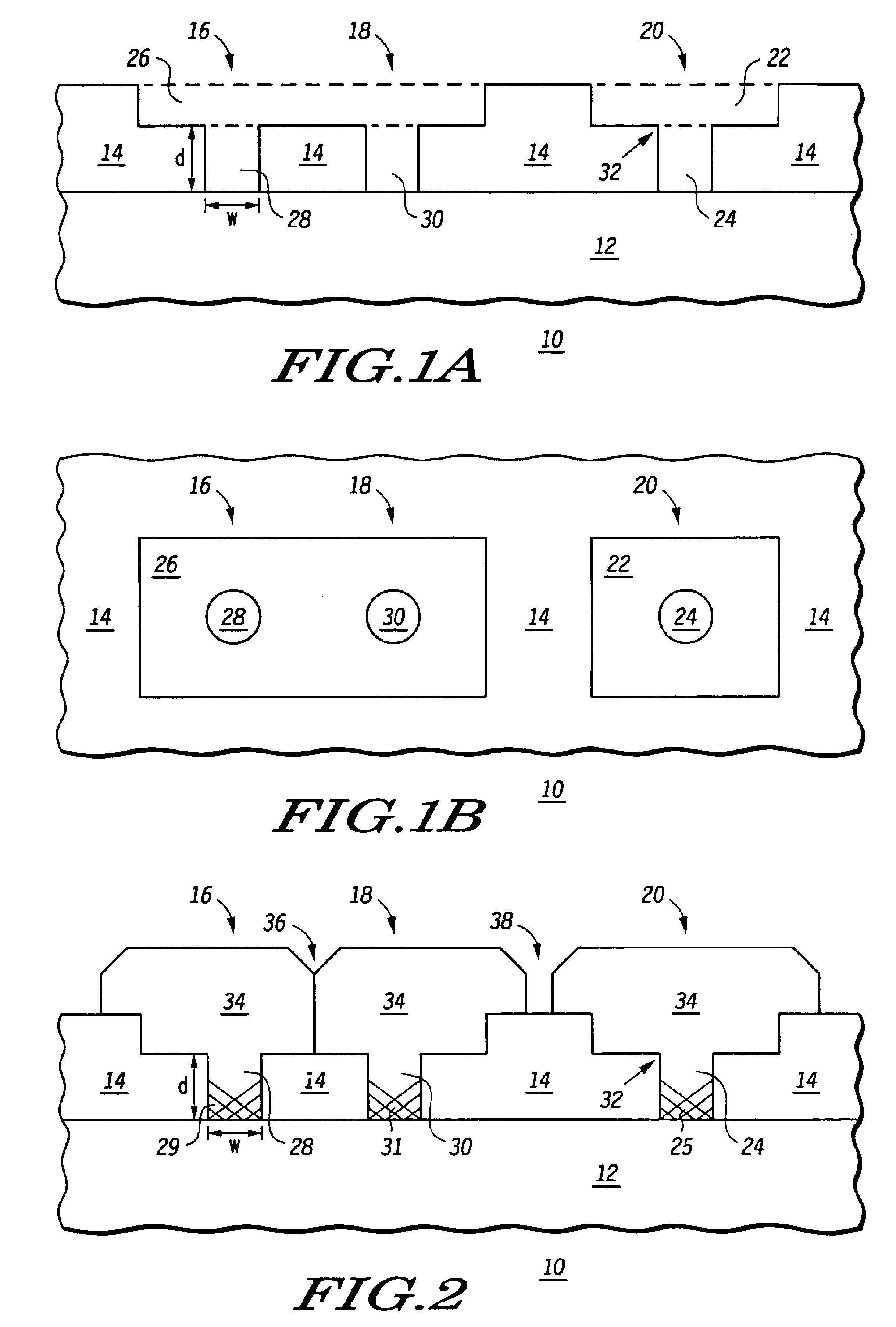
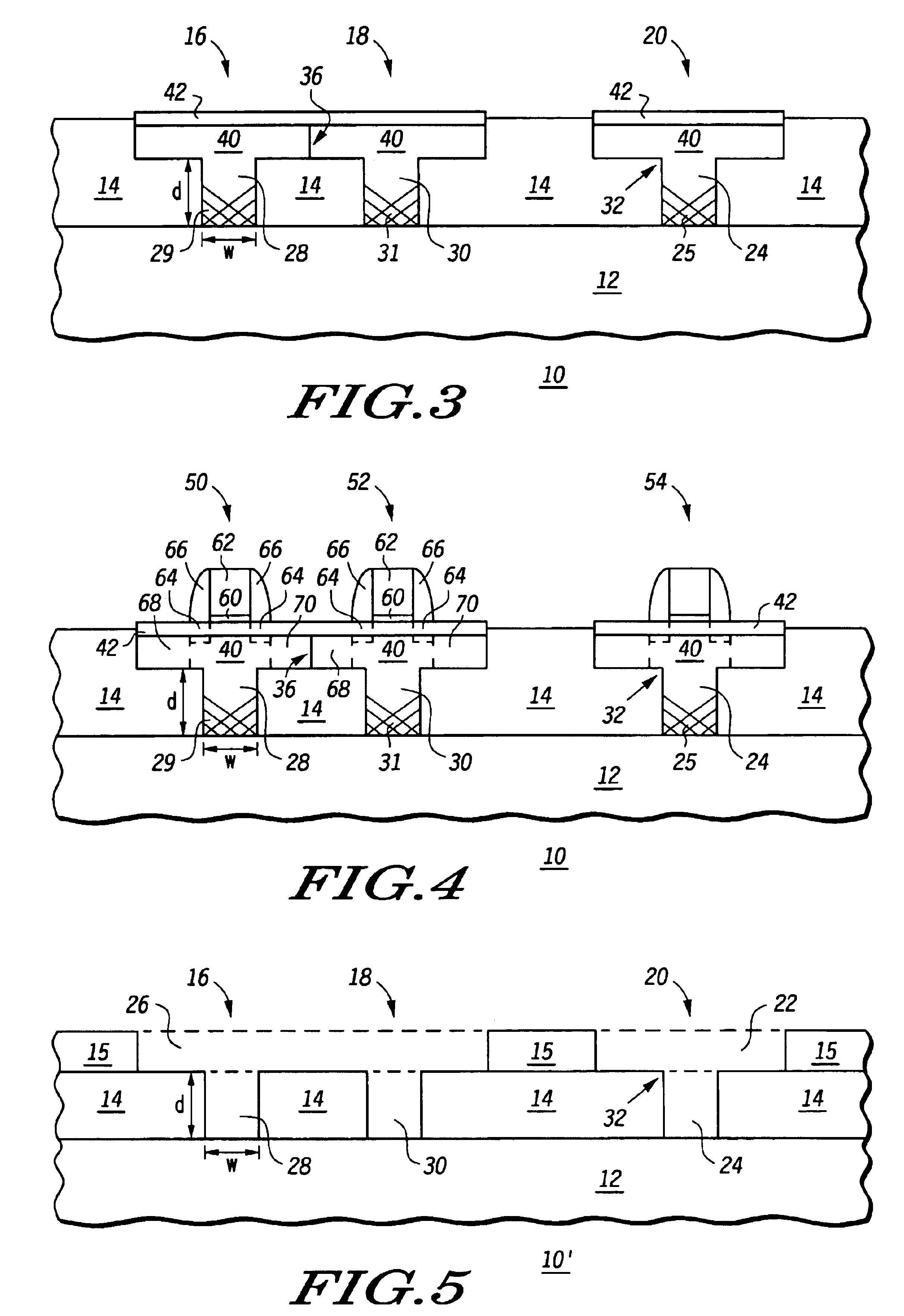
[0016]FIGS. 1-3 are cross-sectional views of various stages in a process of making a semiconductor device incorporating a defect controlled strained channel structure according to an embodiment of the present disclosure. As shown in FIG. 1A, semiconductor device 10 includes a substrate 12 and a dielectric layer 14 overlying the substrate. Substrate 12 includes any single crystal substrate, for example, a bulk silicon substrate, an SOI substrate, silicon on sapphire, or the like. Dielectric layer 14 includes any suitable dielectric layer, for example, a silicon dioxide, oxides, nitrides, or the like.

[0017]Locations of defect controlled strained channel structures, yet to be fabricated, are shown in FIGS. 1A and 1B as indicated by reference numerals 16, 18, and 20. An active region opening 22 is disposed over a substrate via 24, in location 20. Similarly, an active region opening 26 is disposed over both substrate vias 28 and 30, corresponding to locations 16 and 18, respectively. FIG...


PUM


Abstract

A semiconductor device includes a single crystal substrate and a dielectric layer overlying the substrate. The dielectric layer includes at least one opening having a first portion and an overlying second portion. The first portion has a depth and width, such that an aspect ratio of the depth to width is greater than one. The semiconductor device further includes a first material having a first portion and a second portion, the first portion of the first material filling the first portion of the at least one opening. Defects for relaxing strain at an interface between the first material and the substrate material exist only within the first portion of the first material due to the aspect ratio being greater than one. The second portion of the first material is substantially defect free. Furthermore, the second portion of the first material and an overlying second material different than the first material fill the overlying second portion of the at least one opening. The second material has a thickness which is less than a critical thickness to maintain the second material in a strained state. The strained second material functions as a channel for charge carriers.

Description

RELATED APPLICATION[0001]This is related to U.S. patent application Ser. No. 10 / 677,844 filed concurrently herewith, and entitled “Semiconductor Structure with Different Lattice Constant Materials and Method for Forming the Same”, now U.S. Pat. No. 8,831,350 and is incorporated herein by and assigned to the current assignee hereof.BACKGROUND[0002]1. Field of the Invention[0003]The present invention relates generally to semiconductor devices and method of making the same, and more particularly, to a semiconductor device incorporating a defect controlled strained channel structure and method of making the same.[0004]2. Related Art[0005]In the manufacture of semiconductor devices, various isolation structures for CMOS and methods of fabrication are known. One type of isolation structure includes inverse slope isolation. With respect to inverse slope isolation, it possesses a high probability of not terminating defects, for example, from the deposition of SiGe on Si, on a sidewall of th...

Claims


Application Information

Patent Timeline
Patent Type & Authority Patents(United States)
IPC IPC(8): H01L21/336H01L29/06H01L21/02H01L29/10H01L29/02H01L21/762H01L21/8238
CPCH01L21/76262H01L21/823807H01L21/823878H01L29/0653H01L29/1054H01L29/66651
Inventor GRANT, JOHN M.STEPHENS, TAB A.
Owner MOTOROLA INC
Why Eureka
Try Eureka