Broadband PIN diode attenuator bias network

a pin diode attenuator and bias network technology, applied in the field of signal attenuators, can solve the problems of unpredictability and/or undesired operation of particular components, failure to maintain a proper impedance match, and greatly affect the system frequency response (power transfer) and noise figure, and achieve the effect of increasing the complexity of the attenuator control circuitry, reducing the cost of operation, and increasing the dynamic rang

Inactive Publication Date: 2005-07-19
CSR TECH INC
View PDF12 Cites 17 Cited by
  • Summary
  • Abstract
  • Description
  • Claims
  • Application Information

AI Technical Summary

Benefits of technology

[0011]A preferred embodiment PIN diode attenuator is provided by connecting the PIN diodes in a π network. Preferably, the cathodes of all PIN diodes in the π network are DC grounded, such as through large value inductors coupling the cathodes to a DC ground, providing a common cathode point bias voltage which is constant. The preferred embodiment arrangement provides for control current to be applied to the π network shunt diodes and series diode(s) separately. Accordingly, although the complexity of the attenuator control circuitry is increased by the preferred embodiment multiple control current configuration, this configuration allows control of diode currents independently of each other and, therefore, at any given point the preferred embodiment attenuator circuit may be optimized both for insertion loss and return loss. Moreover, controllable attenuators of the present invention provide a large dynamic range. PIN diode attenuators of the present invention have been proven to exceed 35 dB of attenuation range, while maintaining a return loss better than 16 dB.
[0012]Alternative embodiments of the present invention provide a PIN diode attenuator by connecting the PIN diodes in a bridge T network. Preferably, the cathodes of all PIN diodes in the T network are DC grounded, such as through a large value inductor coupling the cathodes to a DC ground, providing a common cathode point bias voltage which is constant. As with the preferred embodiment π network discussed above, the preferred embodiment T network arrangement provides for control current to be applied to the T network shunt diode and series diodes separately. Accordingly, although the complexity of the attenuator control circuitry is increased by the this multiple control current configuration, this configuration allows control of diode currents independently of each other and, therefore, at any given point the preferred embodiment attenuator circuit may be used to optimize its insertion loss and return loss.

Problems solved by technology

For example, often in RF systems, such as CATV cable television systems, RF signal levels vary significantly resulting in unpredictable and / or undesired operation of particular components thereof, such as receivers, tuners, repeaters, and the like.
Failure to maintain a proper impedance match can greatly affect the system frequency response (power transfer) and noise figure.
However, prior art linear attenuators generally provide a tradeoff with respect to these desirable attributes and, therefore, often provide less than ideal operation in demanding system applications.
Similarly, previous attenuation circuit implementations have experienced a trade off between providing attenuation that is a linear function of the control input and providing a low insertion loss.
However, PIN diode attenuator configurations, such as those described above, have heretofore been unable to adequately address such requirements.
For example, previously known bridge T attenuator structures are precluded for use in the above conditions as 30 dB of dynamic range are not available with commercially available PIN diodes in the prior art bridge T network configurations.
Similarly, previously known π attenuator structures, although perhaps able to achieve a relatively large dynamic range, generally are not able to maintain the return loss or impedance match over this dynamic range.
For example, typical prior art π attenuator structures result in poor return loss with designs with greater than 15 dB of attenuation range.

Method used


Image

  • Broadband PIN diode attenuator bias network
  • Broadband PIN diode attenuator bias network
  • Broadband PIN diode attenuator bias network

Examples


Embodiment Construction

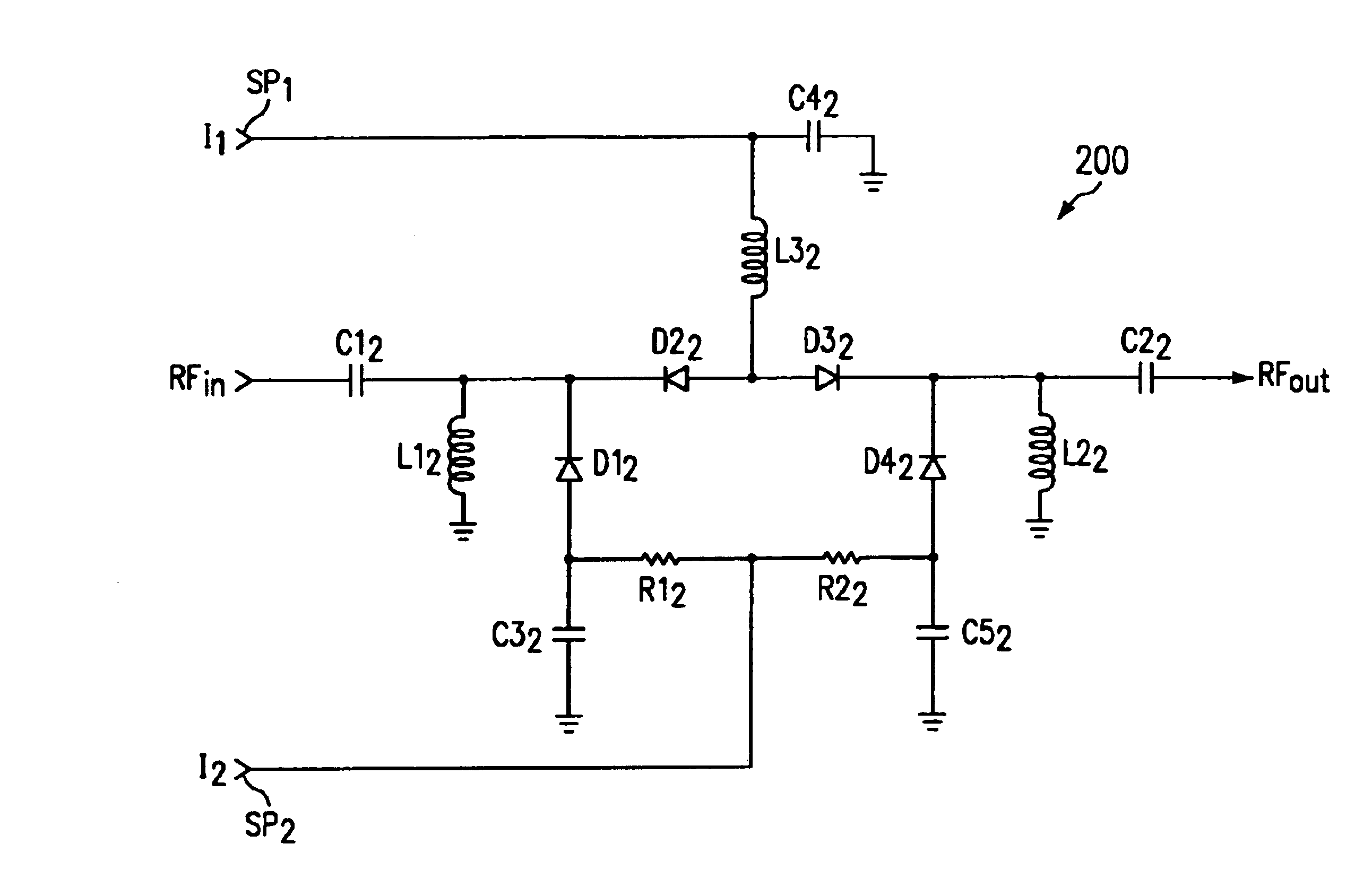
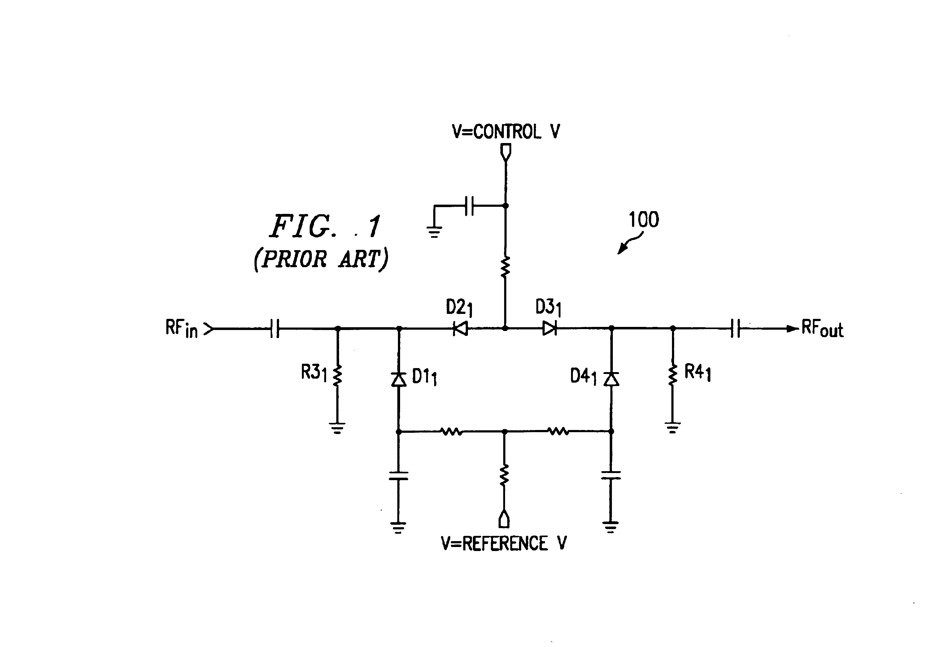
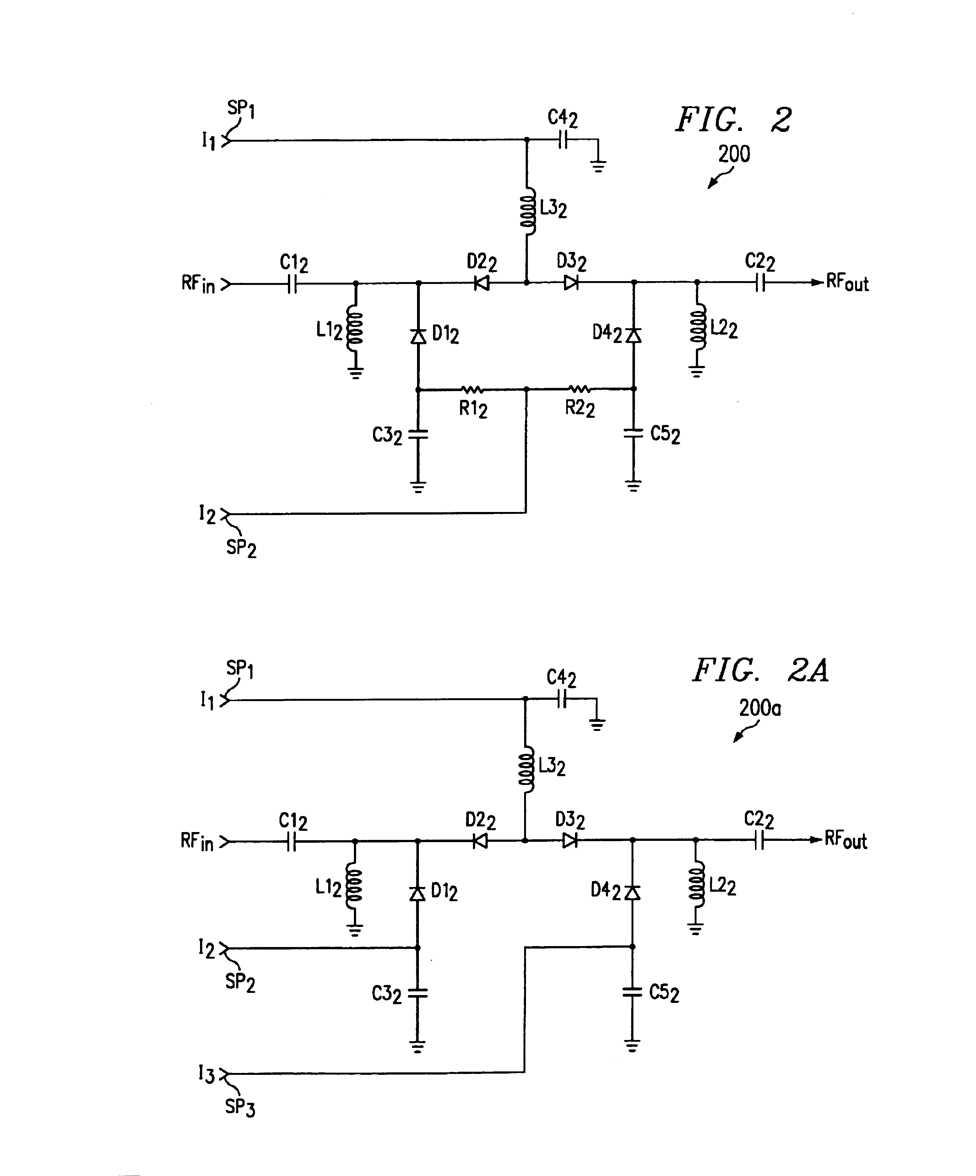
[0020]A discussion of a typical prior art PIN diode attenuator circuit is helpful in understanding the present invention. Directing attention to FIG. 1, a typical prior art PIN diode attenuator circuit is shown as attenuator 100. PIN diodes exhibit a variable RF resistance that is inversely proportional to the DC current through the diode. The design of attenuator 100 requires arranging the PIN diodes to form a suitable RF attenuator network while providing DC bias current to each of the PIN diodes. Accordingly, attenuator 100 includes two PIN diodes arranged in a common cathode configuration (diodes D11 and D21) which are mirrored (diodes D31, and D41) to form a configuration commonly referred to as a π network.

[0021]The common cathode nodes of attenuator 100 are coupled to a DC ground (whether zero potential ground or some potential with respect thereto) through resistors (R31 for the common cathode node of D11 and D21 and R41 for the common cathode node of D31 and D41). Resistors...


PUM


Abstract

Diode network configurations are disclosed in which cathode bias voltage is held substantially constant to provide an attenuator circuit in which return loss is optimized throughout a broad dynamic attenuation range. Preferred embodiments include PIN diodes arranged in a π network having two attenuation control signals provided thereto. Alternative embodiments include PIN diodes arranged in a T network having two attenuation control signals provided thereto.

Description

RELATED APPLICATIONS[0001]The present application is related to concurrently filed commonly assigned United States patent application Ser. No. [49581-P029US-10103788] entitled “Linearizer for a PIN Diode Attenuator,” the disclosure of which is hereby incorporated herein by reference.TECHNICAL FIELD[0002]The invention relates generally to signal attenuators and, more particularly, to a controllable attenuator using positive-intrinsic-negative (PIN) diodes.BACKGROUND[0003]A common requirement in radio frequency (RF) circuits is the control of RF signal levels. For example, often in RF systems, such as CATV cable television systems, RF signal levels vary significantly resulting in unpredictable and / or undesired operation of particular components thereof, such as receivers, tuners, repeaters, and the like. Accordingly, such systems often utilize controllable signal attenuators, such as at the input stage of one of the aforementioned components, in order to provide a relatively constant ...

Claims


Application Information

Patent Timeline
Patent Type & Authority Patents(United States)
IPC IPC(8): H03H7/25H03H7/24
CPCH03H7/255
Inventor RITCHEY, CAREYDAVIS, TOM L.
Owner CSR TECH INC
Why Eureka
Try Eureka