Semiconductor memory

a technology of semiconductor devices and memory cells, applied in semiconductor devices, digital storage, instruments, etc., can solve the problems of increasing wiring resistance, difficult to shorten the maximum read time and reduce the maximum electromagnetic noise generated, and the threshold voltage of each memory cell is disadvantageously changed

Inactive Publication Date: 2005-08-02
KIOXIA CORP
View PDF13 Cites 127 Cited by
  • Summary
  • Abstract
  • Description
  • Claims
  • Application Information

AI Technical Summary

Benefits of technology

[0041]the pass voltage applied to the control electrode of each of said unselected memory cells

Problems solved by technology

Further, since data is read according to the quantity of charges which pass the current terminals of the memory cells, the apparent threshold voltage of each memory cell disadvantageously changes.
On the other hand, when the same logical value is read, if the read current of the memory cell greatly changes according to the position of the memory cell and the data of the unselected memory cells, it is difficult to shorten maximum read time and to reduce the maximum electromagnetic noise generated by the cell current.
In addition, since the maximum current flowing through the data transfer line increases, the rise of wiring resistance and the deterioration of reliability due to electro-migration caused by current stress, the change of the threshold voltage of the transistor and the increase of leakage current following the increase of heat emission disadvantageously occur.
As a result, t

Method used


Image

  • Semiconductor memory
  • Semiconductor memory
  • Semiconductor memory

Examples


first embodiment

[First Embodiment]

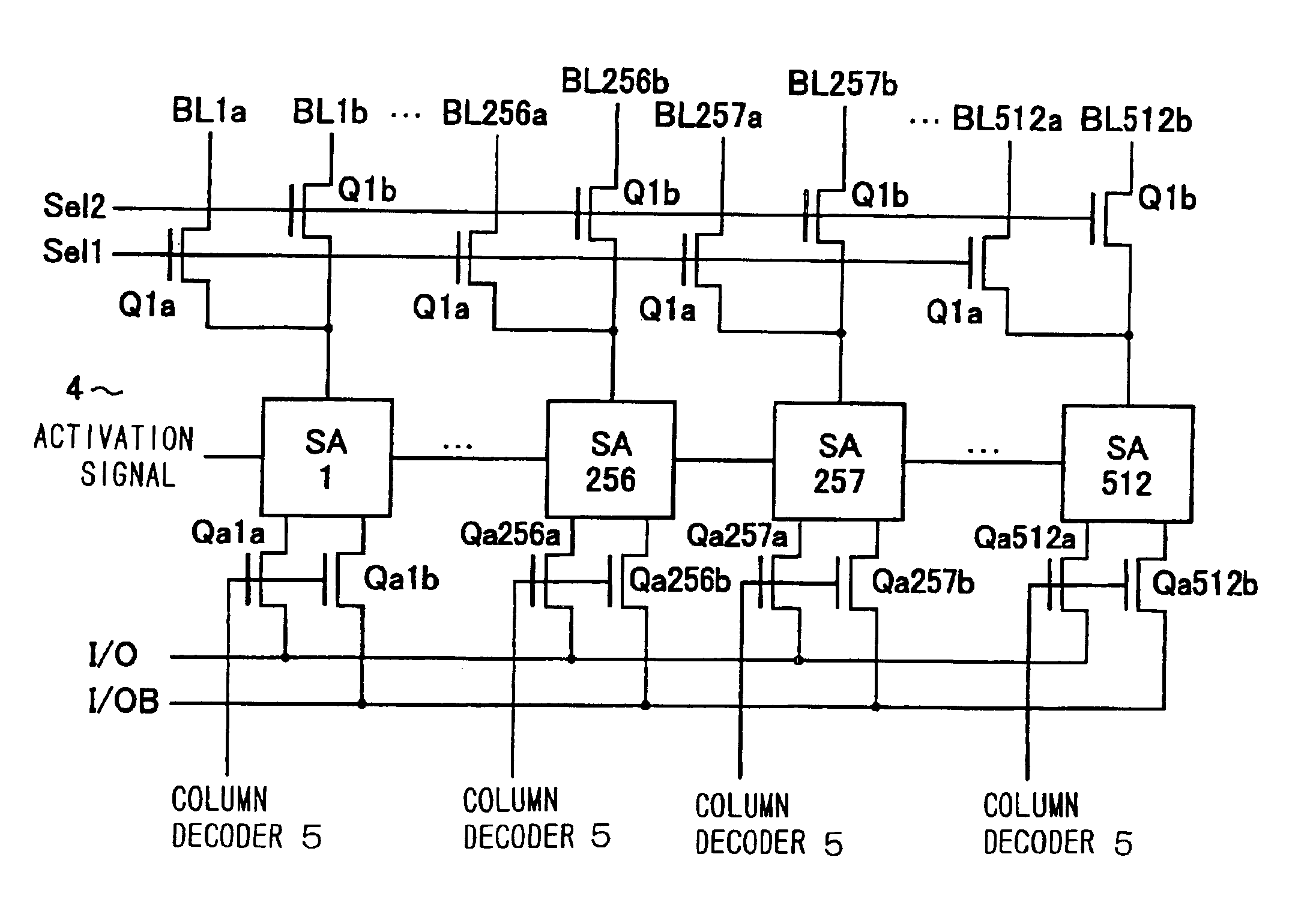
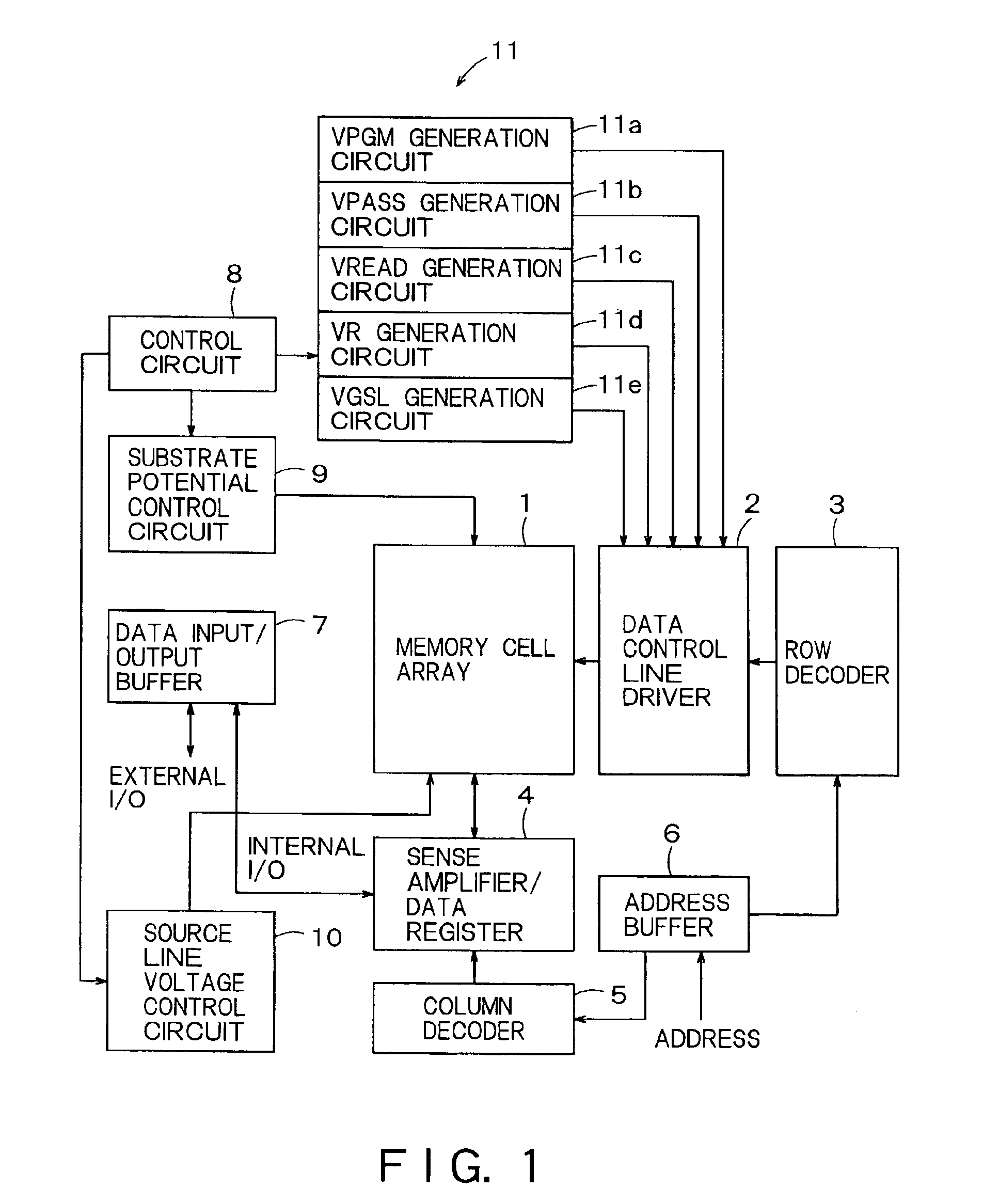
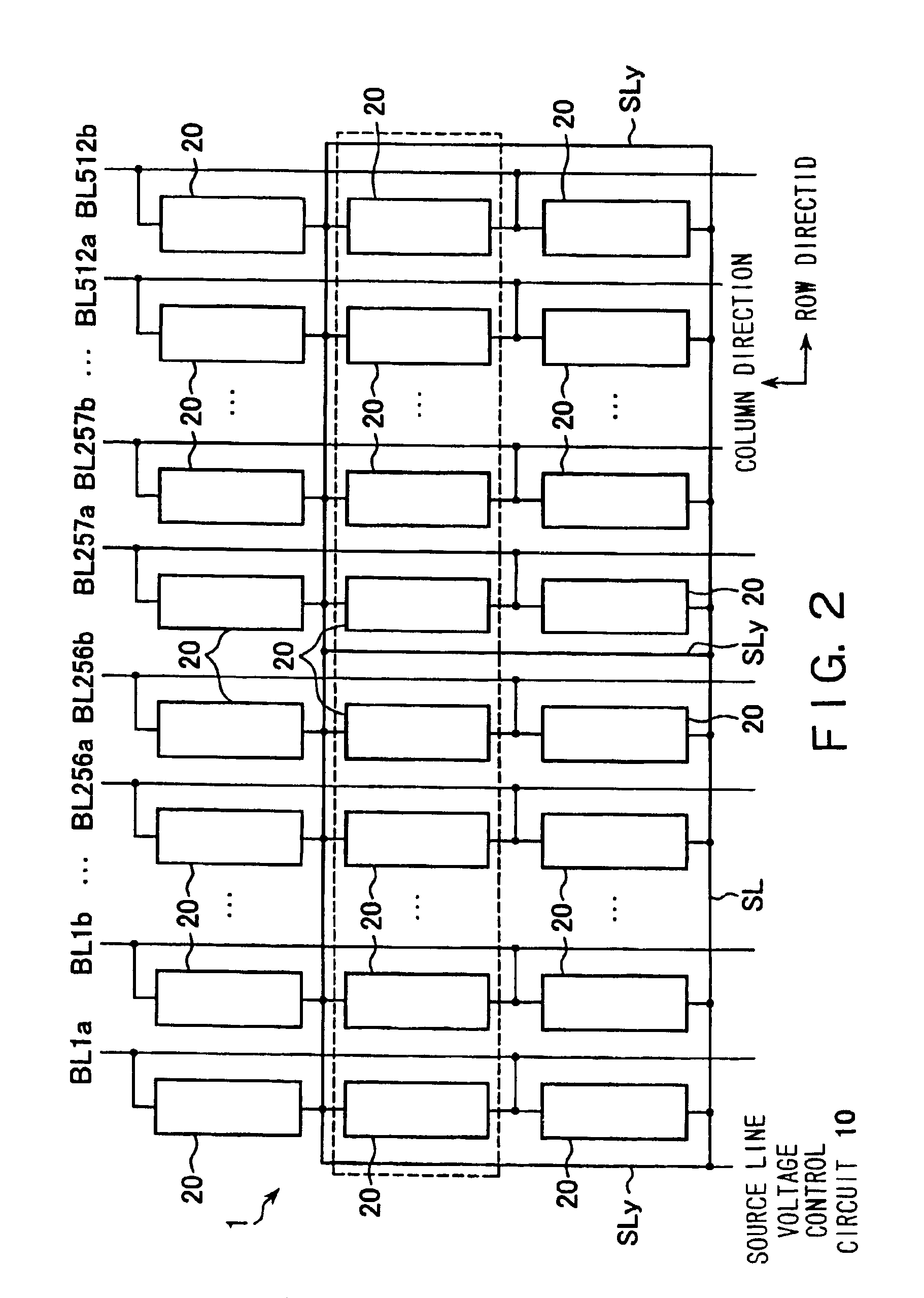
[0088]FIG. 1 shows the configuration of a NAND type EEPROM in the first embodiment. FIG. 2 shows the configuration of a memory cell array of the NAND type EEPROM shown in FIG. 1. The memory cell array 1 is constituted so that a plurality of memory cell units (that is, NAND cell units) 20 each of which includes a plurality of memory cells connected in series, are arranged in row and column directions, respectively. Each NAND cell unit 20 is connected between a data transfer line (to be referred to as “bit line” hereinafter) BL continuous in the column direction and a reference potential line (to be referred to as “common source line” hereinafter) continuous in the row direction. A sense amplifier 4 is provided to sense data of the bit line of the memory cell array 1 or to hold written data. The sense amplifier 4 also serves as a data register and mainly consists of a flip-flop circuit.

[0089]The sense amplifier 4 is connected to a data input / output buffer 7. The conn...

second embodiment

[Modification of Second Embodiment]

[0205]FIGS. 21 and 22 show operation waveforms and voltage relationship if a read current is carried from the common source line to the bit line as the modification of the second embodiment, and correspond to FIGS. 15 and 16, respectively. In FIGS. 21 and 22 as in the case of FIGS. 15 and 16, a case of selecting the word line WL0 is shown and a case of reading data from the memory cell M15 instead of the memory cell M0 is shown in brackets. Data can be read from the other memory cells M1 to M14 by the same operation as that for the memory cell M0.

[0206]During data read, the row decoder 3 and the data control line driver 2 of the data read target block are activated, the read voltage Vr is applied to the selected word line WL0, the pass voltage Vread is applied to each of unselected word lines WL1 to WL15 and the pass voltage Vread is applied to the select gate line SSL (at time t1). The lines SSL, WL0 to WL15 and SSL in unselected blocks are kept i...

third embodiment

[Third Embodiment]

[0217]FIGS. 23 and 24 show the structure of a memory cell array in the third embodiment of the present invention. In this embodiment, not a floating gate type but a MONOS type memory cell structure is employed. The plan view of the cell array is the same as that shown in FIG. 4B. FIGS. 23 and 24 are cross-sectional views taken along lines A-A′ and B-B′ of FIG. 4B, respectively.

[0218]The cell array is formed in a p type well 23 which is formed in the n type well 22 of a p type silicon substrate 21. The boron density of the p type well 23 is set to fall within a range between, for example, 1014 cm−3 and 1019 cm3. The p type well 23 is isolated from the p type silicon substrate 21 by the n type well 22, so that a voltage can be applied to the p type well 23 independently of the p silicon substrate 21. This can reduce load on the booster circuit and to suppress consumption power during data erasure.

[0219]In this embodiment, the gate insulating film of each of the memor...


PUM


Abstract

A semiconductor memory including a memory cell unit, the memory cell unit comprising: a plurality of memory cells in which each conductance between current terminals changes according to held data, each having a plurality of current terminals connected in series between a first terminal and a second terminal, and each capable of electrically rewriting the data; a first select switching element electrically connecting said first terminal to a data transfer line; and a MISFET serving as a second select switching element connecting said second terminal to a reference potential line, wherein said semiconductor memory has a data read mode for forcing the first and second select switching elements of said memory cell unit into conduction, applying a read voltage for forcing a path between the current terminals into conduction or cut-off according to the data of a selected memory cell, to a control electrode of the selected memory cell, applying a pass voltage for forcing a path between the current terminals into conduction irrespectively of the data of each of the memory cells other than said selected memory cell, to the control electrode of each of the memory cells other than said selected memory cell, and detecting presence and absence or magnitude of a current between said data transfer line and said reference potential line, and in said data read mode, a conductance between current terminals of said MISFET is set lower than a conductance, in the case where the conductance between the current terminals is set to be the lowest, with regards to at least one of the memory cells other than said selected memory cell.

Description

CROSS REFERENCE TO RELATED APPLICATIONS[0001]This application is a division of and claims the benefit of priority under 35 USC §120 from U.S. application Ser. No. 10 / 108,574, filed Mar. 29, 2002 now U.S. Pat. No. 6,819,592, and is based upon and claims the benefit of priority under 35 USC § 119 from Japanese Patent Application Nos. 2201-95512, filed on Mar. 29, 2001 and 2001-383554, filed on Dec. 17, 2001, the entire contents of which are incorporated herein by reference.BACKGROUND OF THE INVENTION[0002]1. Field of the Invention[0003]The present invention relates to a semiconductor memory employing electrically rewritable memory cells. More specifically, the present invention relates to a semiconductor memory which constitutes memory cell units by connecting memory cells in series.[0004]2. Related Background Art[0005]Normally, an EEPROM memory cell has a MISFET structure in which a charge accumulation layer and a control gate are layered. This memory cell stores data in a nonvolatil...

Claims


Application Information

Patent Timeline
IPC IPC(8): G11C16/26G11C16/06H01L27/115G11C16/04H01L21/8247H01L27/10H01L29/788H01L29/792
CPCG11C16/26H01L27/115G11C16/0483H10B69/00G11C16/06
Inventor NOGUCHI, MITSUHIROGODA, AKIRAMATSUNAGA, YASUHIKO
Owner KIOXIA CORP
Why Eureka
Try Eureka