Method of manufacturing semiconductor device with interconnections and interconnection contacts and a device formed thereby

a manufacturing method and technology of interconnection contacts, applied in the field of semiconductor devices, can solve the problems of difficult to obtain a desired profile, complicated formation of reliable interconnection contacts, and large increase in loading capacitance between bit lines, so as to achieve the effect of lowering the loading capacitance between interconnections such as bit lines

Active Publication Date: 2005-08-09
SAMSUNG ELECTRONICS CO LTD
View PDF6 Cites 8 Cited by
  • Summary
  • Abstract
  • Description
  • Claims
  • Application Information

AI Technical Summary

Benefits of technology

[0015]According to embodiments of the present invention, the loading capacitance between interconnections such as bit lines can be lowered. Also, the gaps between the interconnections can be effectively filled with an insulating layer and an interconnection contact can be formed in a self-aligned manner.

Problems solved by technology

However, to manufacture semiconductor devices, misalignment margin must be held at a certain level in a photolithography process.
For this reason, forming reliable interconnection contacts becomes more complicated.
Nevertheless, these new techniques require additional process steps and result in a big increase in loading capacitance between bit lines.
While it is possible to replace silicon nitride spacers with silicon oxide spacers, if this is done, it is difficult to obtain a desired profile.
This also makes it difficult to secure a sufficient distance for electric insulation between bit lines and interconnection contacts.
The increase in loading capacitance, a reduced design rule and a much higher height of a stack of bit lines can cause serious problems.
Thus, if spacers are formed on sides of the bit lines so as to perform an SAC process, it becomes more difficult to fill gaps in an interlayer dielectric formed to insulate bit lines.

Method used


Image

  • Method of manufacturing semiconductor device with interconnections and interconnection contacts and a device formed thereby
  • Method of manufacturing semiconductor device with interconnections and interconnection contacts and a device formed thereby
  • Method of manufacturing semiconductor device with interconnections and interconnection contacts and a device formed thereby

Examples


Embodiment Construction

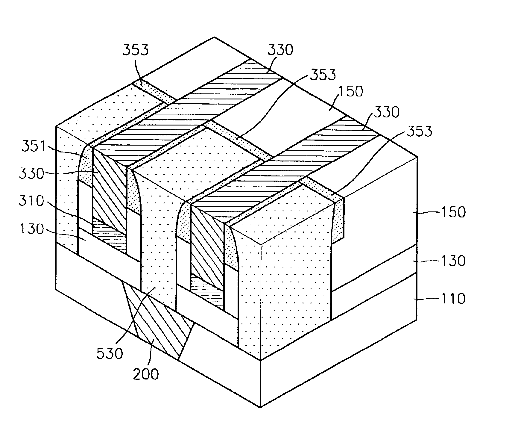
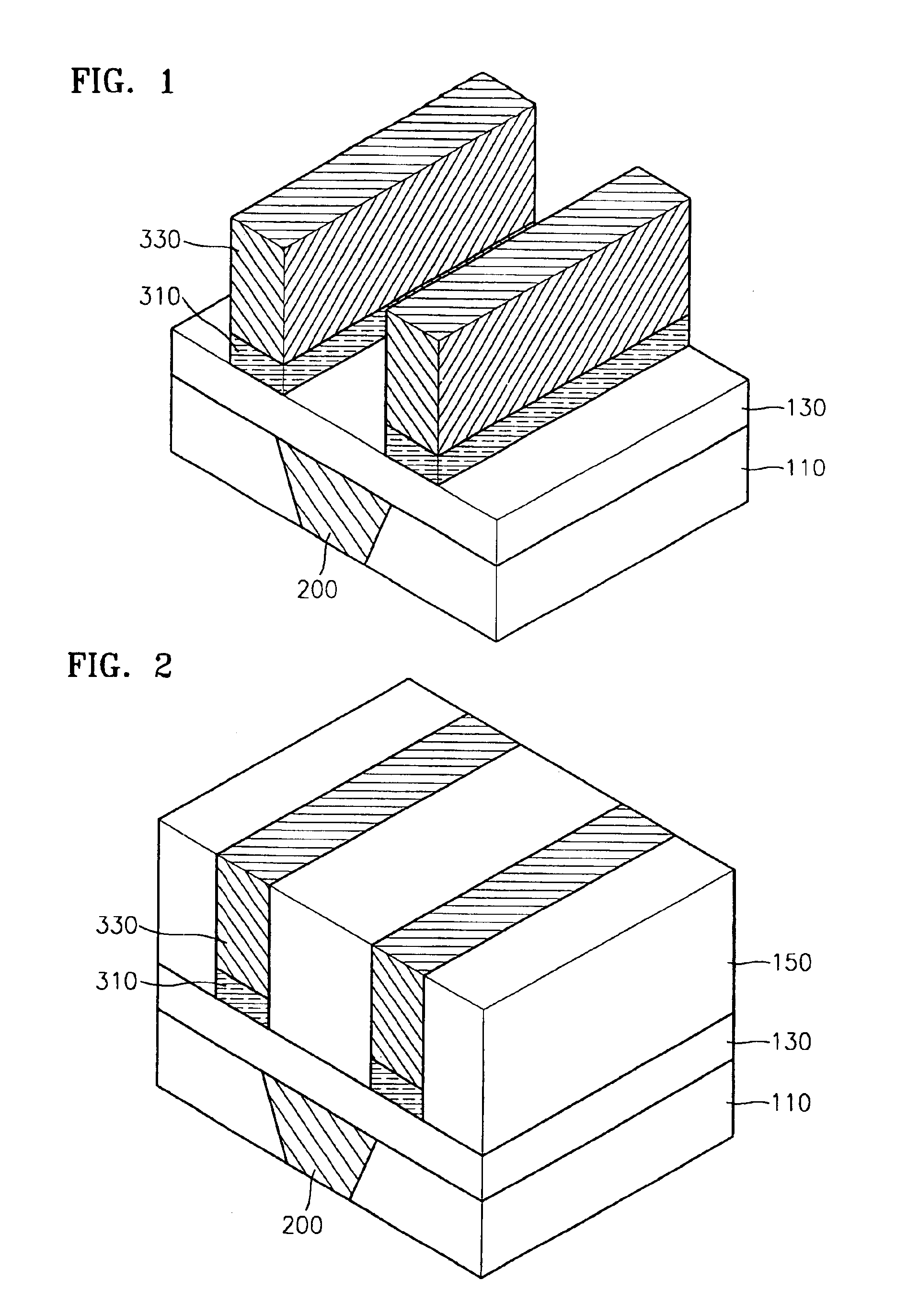
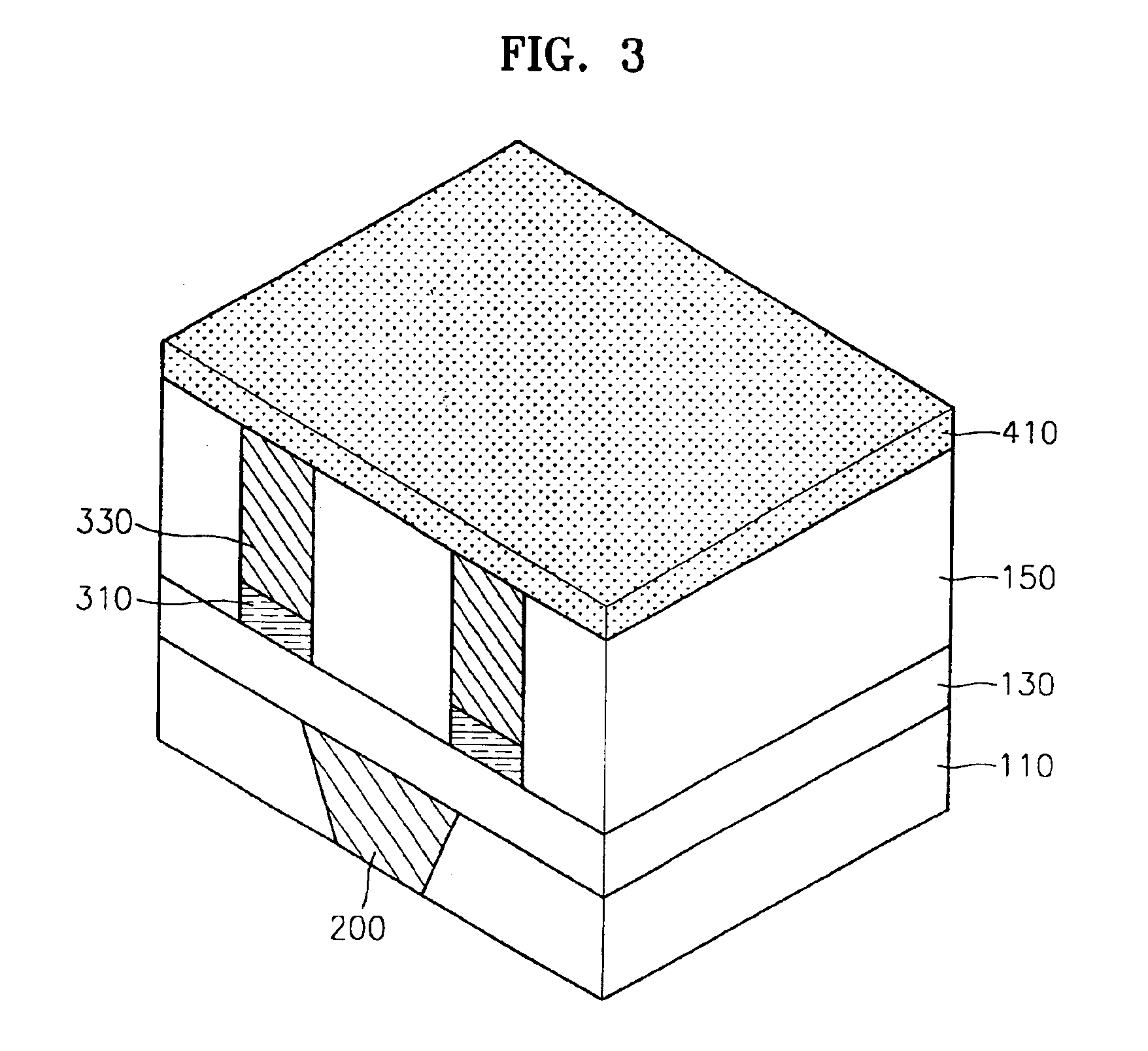
[0028]Embodiments of the present invention will now be described more fully with reference to the accompanying drawings, in which preferred embodiments of the invention are shown. In the embodiments of the present invention, a loading capacitance between interconnections, i.e., bit lines, can be reduced and gaps between the interconnections can be effectively filled with an insulating layer. Also, an interconnection contact can be formed in a self-aligned manner.

[0029]To form the self-aligned interconnection contact with a reduced loading capacitance, a bit line mask is formed on a bit line, and top spacers are formed on upper sides of the bit line mask. Also, to lower the loading capacitance and to enhance a gap filling characteristic of an insulating layer, the bit line mask is formed and then gaps between bit lines are filled with an insulating layer before spacers are formed.

[0030]Also, when the gaps between the bit lines are selectively opened to form the top spacers and an int...


PUM


Abstract

A second insulating layer is formed on a first insulating layer. A plurality of stacks each including a bit line and a bit line mask are formed on the second insulating layer. A third insulating layer is formed overlying the second insulating layer to fill gaps between the plurality of stacks. A hard mask layer is formed on the third insulating layer. A photoresist pattern is formed on the hard mask layer. The photoresist pattern has an opening region that intersects the plurality of stacks. The hard mask layer and the third insulating layer are sequentially etched, using the photoresist pattern as an etching mask, thereby forming a hard mask pattern and forming a recess in the third insulating layer. The recess exposes a portion of upper sidewalls of the bit line mask. Spacers are formed on the exposed upper sidewalls of the bit line mask.

Description

[0001]This application claims the priority of Korean Patent Application No. 2003-28004, filed on May 1, 2003, in the Korean Intellectual Property Office, the disclosure of which is incorporated herein by reference in their entirety.BACKGROUND OF THE INVENTION[0002]1. Field of the Invention[0003]The present invention relates to semiconductor devices, and more particularly, to a method of manufacturing a semiconductor device with interconnection contacts, which are formed by perpendicularly penetrating an insulating layer disposed between interconnections such as bit lines and to a device formed thereby.[0004]2. Description of the Related Art[0005]As semiconductor devices become more highly integrated, design rules are being scaled down. In particular, the contact size of DRAMs is decreasing with a higher integration density of semiconductor devices. However, to manufacture semiconductor devices, misalignment margin must be held at a certain level in a photolithography process. For th...

Claims


Application Information

Patent Timeline
Patent Type & Authority Patents(United States)
IPC IPC(8): H01L21/70H01L21/4763H01L21/8242H01L21/02H01L21/28H01L21/60
CPCH01L21/76897H01L2924/0002H01L2924/00H01L21/76831H01L21/28
Inventor PARK, JE-MINSON, SEUNG-YOUNGHWANG, YOO-SANG
Owner SAMSUNG ELECTRONICS CO LTD
Why Eureka
Try Eureka