CMOS image sensor system with self-reset digital pixel architecture for improving SNR and dynamic range

a digital pixel sensor and image sensor technology, applied in the field of digital pixel sensor architecture, can solve the problems of limited dynamic range, limited readout rate, ccd sensor, etc., and achieve the effects of improving dynamic range and signal-to-noise ratio, improving snr, and extending dynamic rang

Inactive Publication Date: 2005-08-09
THE BOARD OF TRUSTEES OF THE LELAND STANFORD JUNIOR UNIV
View PDF19 Cites 56 Cited by
  • Summary
  • Abstract
  • Description
  • Claims
  • Application Information

AI Technical Summary

Benefits of technology

[0056]It is also an object of the present invention to provide novel CMOS self-reset DPS image sensor apparatuses and systems for increasing SNR without reducing dynamic range.
[0062]Yet another object of the present invention is to provide a method for improving SNR without reducing dynamic range in a CMOS video sensor system with self-reset DPS architecture under low illumination, the method comprising the steps of eliminating global frame reset for the self-reset DPS pixels, capturing and storing a plurality of frames, extending integration time beyond frame readout time, and generating frame images using one or more previously stored frames; the method further comprising steps of determining optimal duration of the extending step by analyzing captured frames and terminating said extending step when dramatic motion is detected thereby preventing severe motion blur.

Problems solved by technology

However, CCD sensors also have many weaknesses, including limited readout rates and limited dynamic range.
The most well known weakness is the difficulty and high costs of integrating CCD image sensors with CMOS-based microprocessors.
CMOS-based integrated circuit (IC) chips containing a CCD image sensor usually have a relatively low yield and are quite expensive because of the specialized processing involved.
For example, as described in above-referenced article, “A 10,000 Frames / s 0.18 μm CMOS Digital Pixel Sensor with Pixel-Level Memory”, achieving acceptable pixel sizes using DPS architecture requires the use of a 0.18 μm or smaller CMOS process, which is challenging due to reduced supply voltages and increased leakage currents.
Unfortunately, CMOS APS image sensors are usually noisier than CCD image sensors.
In other words, CMOS APS image sensors generally suffer from limited dynamic range and poor SNR, limiting their use in most image sensor and higher-end video applications.
This is not desirable.3. The reference voltage supply circuit VDD2 is unstable and thus may trigger false self-reset.
Because the reference voltage supply circuit VDD2 is affected by inverter switching and thus unstable, false self reset may be triggered.4. By adding circuitry to a conventional active pixel cell, this prior art self reset APS architecture provides an undesirably large active pixel cell that still suffers from poor SNR and other drawbacks commonly found in CMOS APS implementations.

Method used


Image

  • CMOS image sensor system with self-reset digital pixel architecture for improving SNR and dynamic range
  • CMOS image sensor system with self-reset digital pixel architecture for improving SNR and dynamic range
  • CMOS image sensor system with self-reset digital pixel architecture for improving SNR and dynamic range

Examples


Embodiment Construction

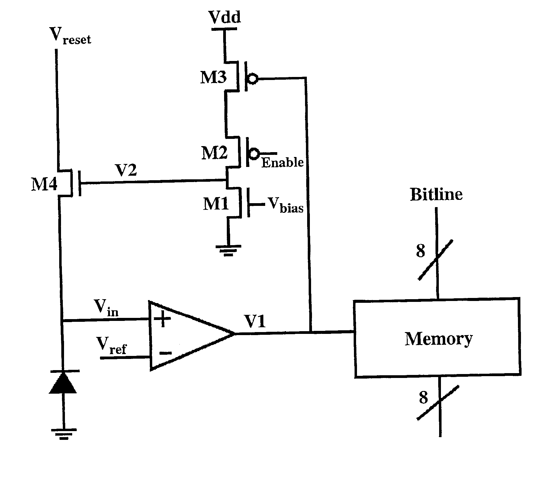
[0072]Analog circuit design in a mixed signal environment has become more and more challenging as the industry migrates to deep submicron regime. For example, signal swing, the most important factor in determining an image sensor's dynamic range and SNR, is dramatically reduced as technology scales. This is especially evident in APS image sensor implementations where, as power supply voltage reduces, the analog signal swing decreases rapidly. With a small analog signal swing and its associated noise, it is extremely hard to get a typical 8-bit image using an on-chip ADC. The situation for DPS image sensors is better because the ADC is usually substantially closer to the signal source.

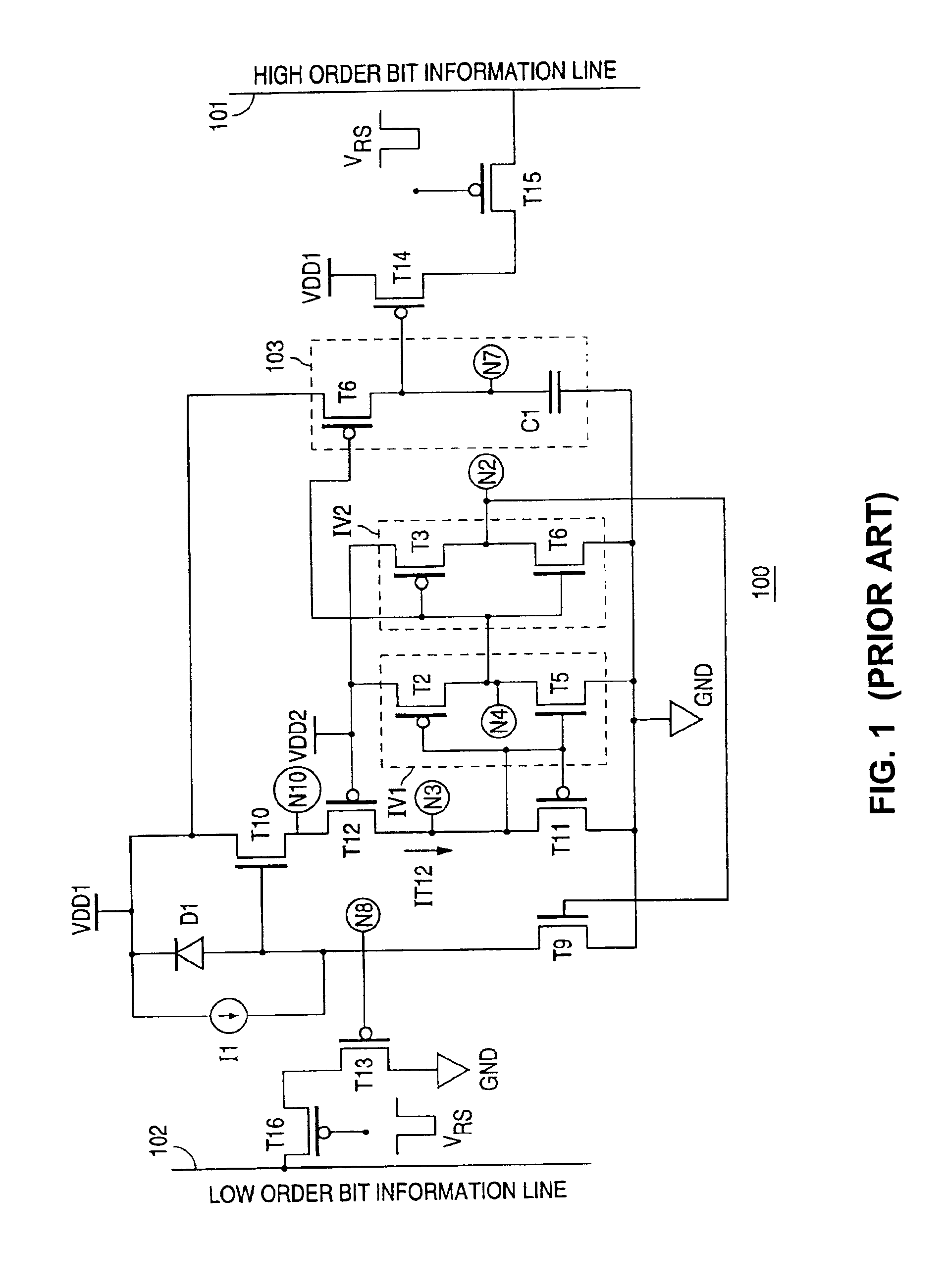
[0073]There are several known implementations providing sensor dynamic range enhancement, including multiple sampling, i.e., capturing multiple pixel samples, as well as well adjustment schemes. However, these implementations suffer drawbacks such as limited application, e.g., only work for still images...


PUM


Abstract

A CMOS DPS image sensor architecture for improving SNR and dynamic range is presented. The CMOS DPS architecture includes self-reset digital pixels capable of collecting more charge than the physical well capacity. A method for improving SNR without reducing dynamic range in a CMOS video sensor system under low illumination is described, wherein the CMOS video sensor system employing self-reset DPS architecture includes pixel level A / D conversion and wherein each DPS pixels is capable of resetting itself whenever a corresponding diode reaches saturation during integration time.

Description

CROSS-REFERENCE TO RELATED APPLICATIONS[0001]This application relates to a co-pending U.S. patent application Ser. No. 09 / 961,847 filed on Sep. 24, 2001 and entitled “METHOD FOR IMPROVING SNR IN LOW ILLUMINATION CONDITIONS IN A CMOS VIDEO SENSOR SYSTEM USING A SELF-RESETTING DIGITAL PIXEL”. This application also relates to U.S. patent application Ser. No. 09 / 992,479, filed on Nov. 13, 2001, entitled “PHOTOCURRENT ESTIMATION FROM MULTIPLE CAPTURES FOR SIMULTANEOUS SNR AND DYNAMIC RANGE IMPROVEMENT IN CMOS IMAGE SENSORS”, and U.S. patent application Ser. No. 09 / 992,480, filed on Nov. 13, 2001, entitled “MOTION / SATURATION DETECTION SYSTEM AND METHOD FOR SYNTHESIZING HIGH DYNAMIC RANGE MOTION BLUR FREE IMAGES FROM MULTIPLE CAPTURES”, all of which are assigned to the same assignee as the present application and are hereby incorporated herein by reference.BACKGROUND OF THE INVENTION[0002]1. Field of the Invention[0003]The present invention relates generally to digital pixel sensor archite...

Claims


Application Information

Patent Timeline
Patent Type & Authority Patents(United States)
IPC IPC(8): H04N3/15H04N5/355H04N5/361H04N5/363H04N5/365H04N5/374
CPCH04N3/155H04N25/533H04N25/772
Inventor LIU, XINQIAOLIM, SUK HWANGAMAL, ABBAS EL
Owner THE BOARD OF TRUSTEES OF THE LELAND STANFORD JUNIOR UNIV
Why Eureka
Try Eureka