Gas discharge tube and method for forming electron emission layer in gas discharge tube

a gas discharge tube and electron emission film technology, which is applied in the manufacture of electric discharge tubes/lamps, cold cathode manufacture, electrode systems, etc., can solve the problems of narrowing the margin of light-emitting operations, difficult to form electron emission films on the inner wall, and non-uniform film thickness distribution in the tube, so as to reduce voltage, uniform thickness, and uniform thickness

Inactive Publication Date: 2005-08-23
SHINODA PLASMA
View PDF9 Cites 46 Cited by
  • Summary
  • Abstract
  • Description
  • Claims
  • Application Information

AI Technical Summary

Benefits of technology

[0014]The present invention is accomplished in view of these circumstances, and aims to improve discharge characteristics and reduce the unevenness of the light-emitting operation among many light-emitting points by forming an electron emission film on the inner wall of a gas discharge tube with a uniform thickness.
[0015]The present invention provides a gas discharge tube comprising a plurality of light-emitting portions that are provided outside of the tube and comprise at least two discharge electrodes, and an electron emission film formed on the entire inner wall of the tube for improving discharge characteristics.
[0016]The gas discharge tube according to the present invention has the electron emission film formed on the entire inner wall of the tube, whereby discharge characteristics is improved upon generating a discharge between discharge electrodes via the gas discharge tube.
[0018]The method for forming an electron emission film according to the present invention comprises a step of injecting coating solution from one opening of a tube at a predetermined amount; a step of forming a coating film on the entire inner wall of the tube by causing the coating solution to trickle down the inner wall of the tube while entirely sealing the opening of the tube and a step of burning the resultant film, whereby an electron emission film having a uniform thickness can be formed on the entire inner wall of the tube. The formation of the electron emission film having a uniform thickness can reduce the voltage for initiating the discharge of the gas discharge tube as well as can widely assure a margin of a light-emitting operation at many light-emitting points.

Problems solved by technology

However, it is extremely difficult to form the electron emission film on the inner wall of the slender, long glass tube having a diameter of 2 mm or less and a length of 200 mm or more.
For example, a film-formation by a vapor deposition method brings a non-uniform distribution of the film thickness in the tube since evaporating molecules of a material for forming an electron emission film introduced from the tube edge is significantly accumulated in the vicinity of the tube edge.
The uneven thickness of the electron emission film causes variations in the voltage for initiating the discharge at a great many of light-emitting points in the tube, thereby arising a problem of narrowing the margin of the light-emitting operation.

Method used


Image

  • Gas discharge tube and method for forming electron emission layer in gas discharge tube
  • Gas discharge tube and method for forming electron emission layer in gas discharge tube
  • Gas discharge tube and method for forming electron emission layer in gas discharge tube

Examples


embodiment

Embodiment 1

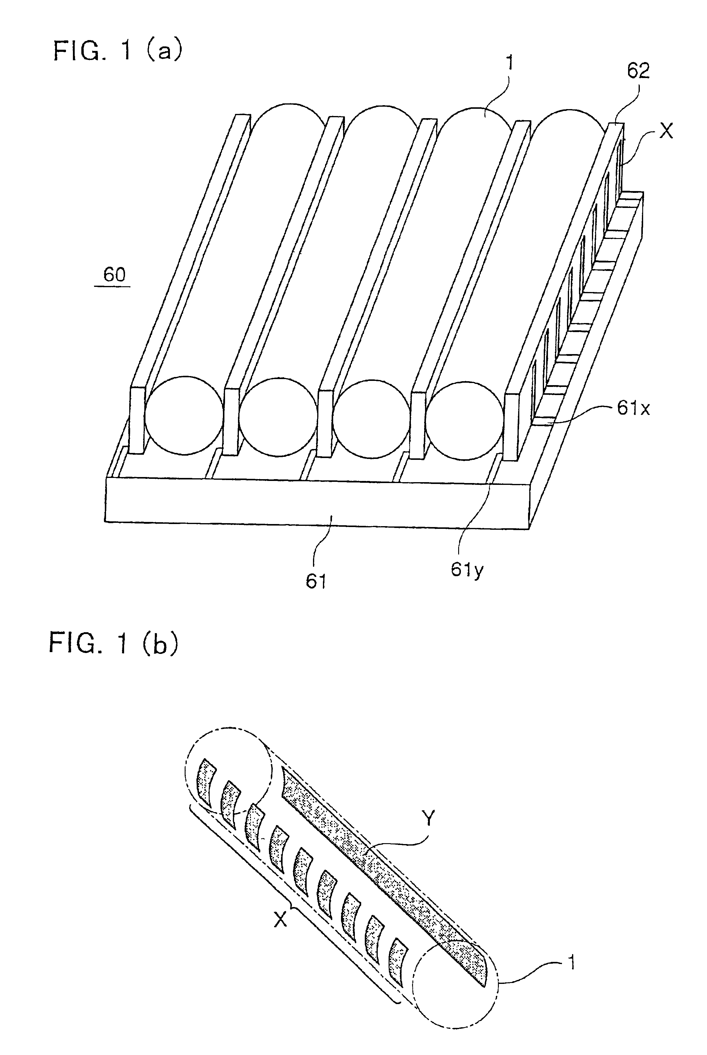
[0087]FIGS. 12(a) to 12(e) are explanatory views showing Embodiment 1 of a method for forming an electron emission film to the inside of the gas discharge tube.

[0088]A gas discharge tube 41 used in this embodiment is made of glass, and has an outer diameter of 1.0 mm, inner diameter of 0.8 mm and length of 200 mm. Magnesium hexanoate is used for an organic metal compound that becomes an electron emission film by burning. Used for the coating solution 42 is the one containing ethanol of 1 part and propylene glycol monomethyl ethyl acetate of 1 part per 1 part of magnesium hexanoate.

[0089]The gas discharge tube 41 is prepared (see FIG. 12(a)), and then, the coating solution 42 is introduced to the edge portion of the gas discharge tube 41 (see FIG. 12(b)). Thereafter, the coating solution 42 is uniformly applied to the inner wall of the gas discharge tube by using a rotating device 43 that is a spinner (see FIG. 12(c)). At this time, the coating solution 42 is applied with...

embodiment 2

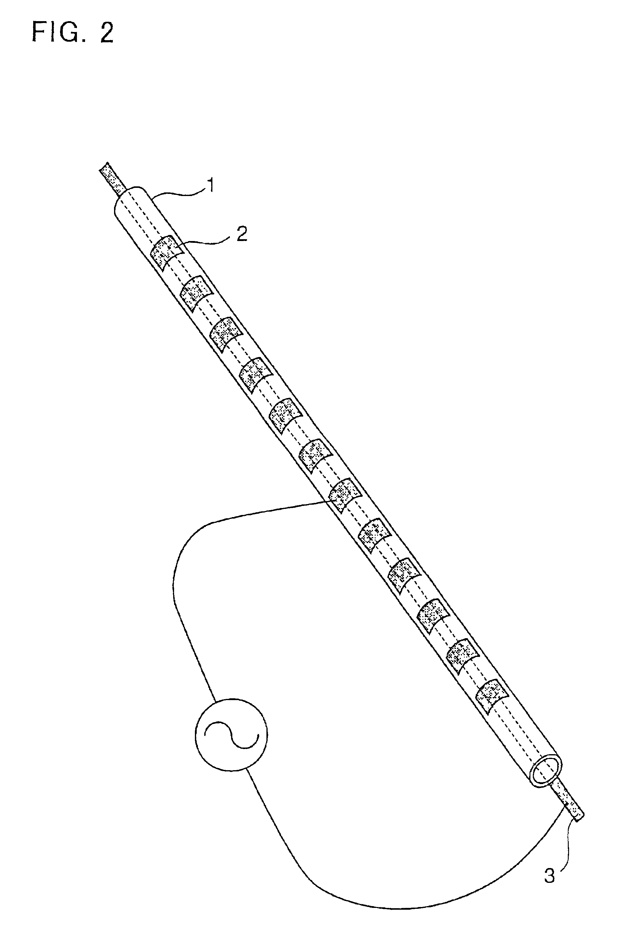
[0093]FIG. 13 is an explanatory view showing Embodiment 2 of a method for forming an electron emission film on the gas discharge tube.

[0094]The gas discharge tube 41 used in this embodiment is also made of glass. This gas discharge tube has an outer diameter of 1.0 mm, inner diameter of 0.8 mm and length of 1000 mm. Magnesium hexanoate is used for an organic metal compound that becomes an electron emission film by burning. Used for the coating solution is the one containing ethanol of 0.5 parts and propylene glycol monomethyl ethyl acetate of 0.8 part per 1 part of magnesium hexanoate.

[0095]The coating solution 47 is introduced into a gas discharge tube 46 for filling the tube, and then, the coating solution 47 is moved by a roller pump 48 at a speed of 50 mm per minute, to thereby apply the coating solution 47 onto the inner wall of the gas discharge tube 46. The coated portion is subject to an infrared ray lamp 49 for obtaining a dried coating film. A shielding plate 50 is moved w...


PUM


Abstract

A gas discharge tube includes a plurality of light-emitting portions that are provided outside of the tube, at least two discharge electrodes, and an electron emission film formed on the entire inner wall of the tube for improving discharge characteristics.

Description

CROSS-REFERENCES TO RELATED APPLICATIONS[0001]This application is related to Japanese applications No. 2001-232449 filed on Jul. 31, 2001, whose priority is claimed under 35 USC §119, the disclosures of which are incorporated by reference in their entirety.BACKGROUND OF THE INVENTION[0002]1. Field of the Invention[0003]The present invention relates to a gas discharge tube and a method for forming an electron emission film into the gas discharge tube, and more particularly to a thin gas discharge tube having a diameter of approximately 0.5 to 5 mm and a method for forming an electron emission film into the gas discharge tube suitably adapted for such a gas discharge tube.[0004]2. Description of the Related Arts[0005]A conventional gas discharge tube is provided with electrodes at end edges with respect to the longitudinal direction of the discharge tube for extending a discharge in the longitudinal direction. Films of an electron emission material (electron emission film) that improv...

Claims


Application Information

Patent Timeline
Patent Type & Authority Patents(United States)
IPC IPC(8): H01J61/04H01J61/06H01J9/02H01J65/04H01J9/20H01J37/32H01J61/54H01J65/00
CPCH01J9/02H01J61/04H01J61/06H01J65/046H01J37/32
Inventor YAMADA, HITOSHITOKAI, AKIRAISHIMOTO, MANABUSHINODA, TSUTAE
Owner SHINODA PLASMA
Why Eureka
Try Eureka