Method and system for flip chip packaging
- Summary
- Abstract
- Description
- Claims
- Application Information
AI Technical Summary
Benefits of technology
Problems solved by technology
Method used
Image
Examples
Embodiment Construction
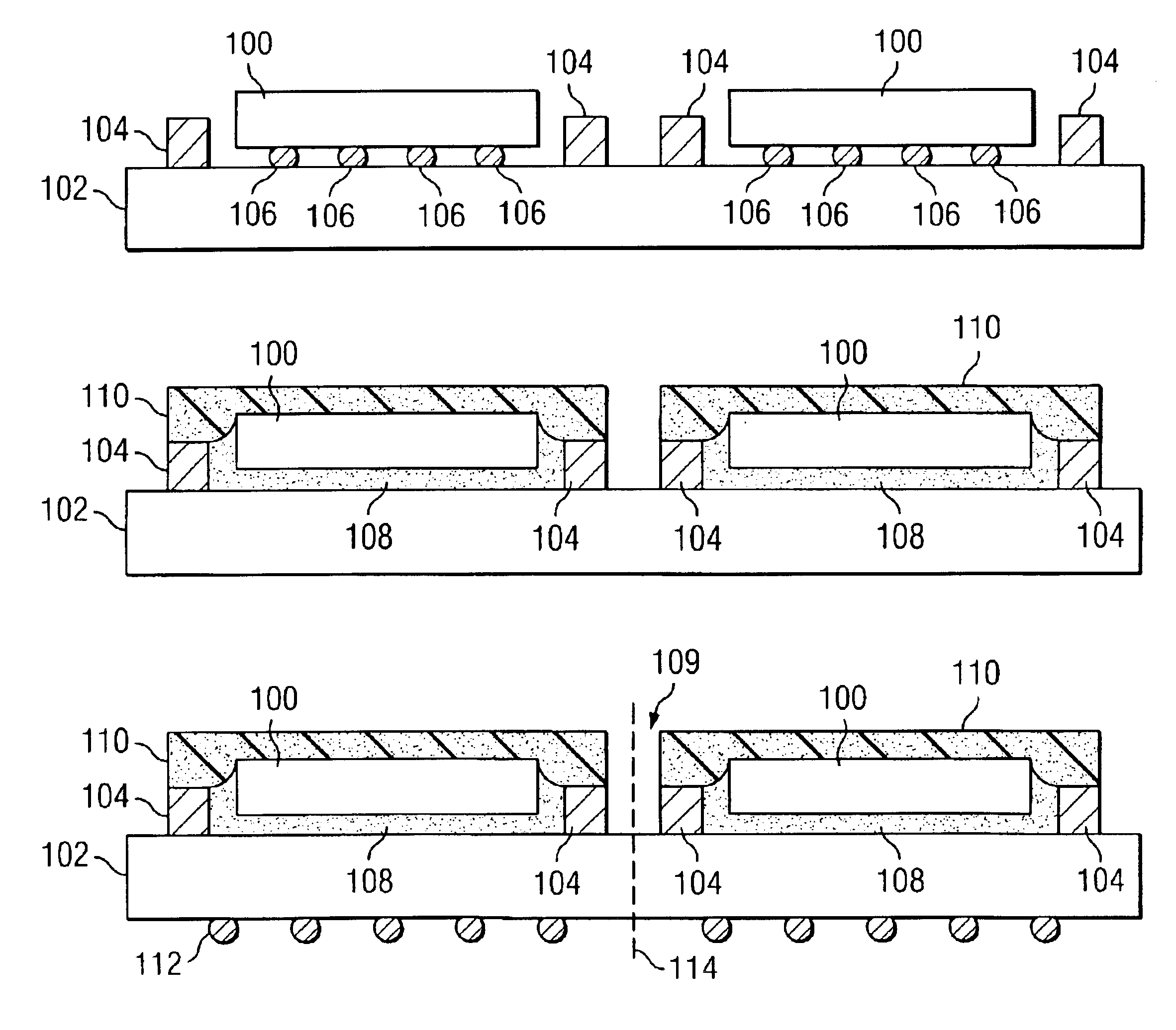
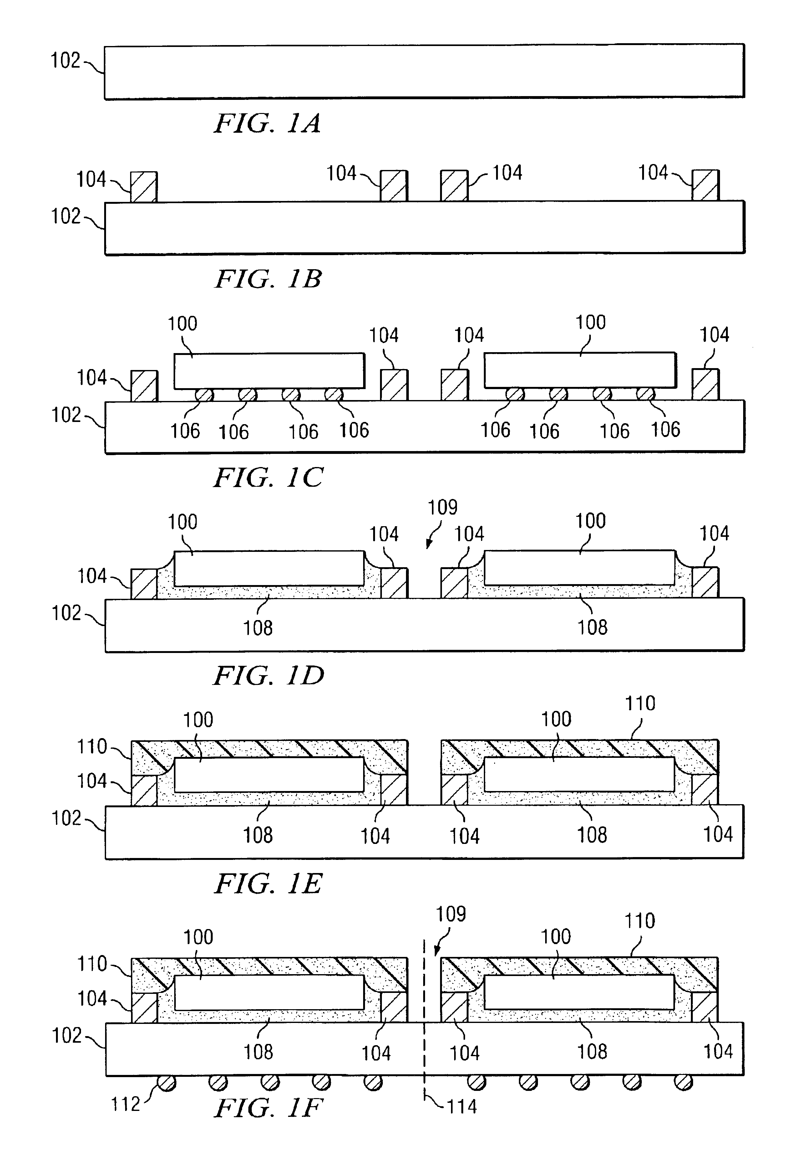
[0008]Example embodiments of the present invention and their advantages are best understood by referring now to FIGS. 1A through 1F of the drawings, in which like numerals refer to like parts.
[0009]FIGS. 1A through 1F are a series of cross-sectional elevation views illustrating an example method of packaging a plurality of flip chips 100 (FIG. 1C) in accordance with an embodiment of the present invention. Flip chip packaging is generally more expensive than wire bond packaging. Therefore, one way to reduce the cost of flip chip packaging is to package a high number of closely spaced flip chips on a given panel or substrate. In the example illustrated in FIG. 1A, a panel 102 may be used to package a plurality of closely spaced flip chips, such as flip chips 100.
[0010]Panel 102, in one embodiment, is a glass-fiber-reinforced epoxy resin, such as FR4; however, panel 102 may be formed from other suitable materials. For example, panel 102 may be formed from thinner substrates, such as po...
PUM
 Abstract
Description
Claims
Application Information

