

Leadless plastic chip carrier with etch back pad singulation
Inactive Publication Date: 2005-08-23
UTAC HEADQUARTERS PTE LTD
View PDF29 Cites 161 Cited by
- Summary
- Abstract
- Description
- Claims
- Application Information
AI Technical Summary
Benefits of technology
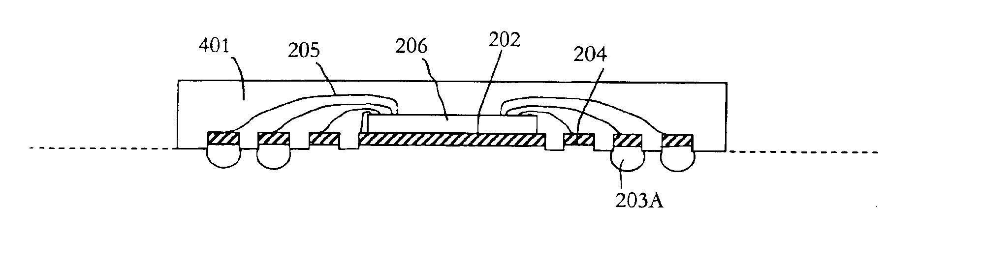
[0008]According to the present invention, Applicant's etch-back LPCC process has been modified to provide additional design features. Firstly, an etch barrier is provided as the first layer of the contact pads and die attach pad, and the contact pads are formed to a “rivet” head shape for improved interlocking and the die attach pad is formed with an interlock pattern for improved alignment with the semiconductor die. Improved electrical performance is enjoyed over the above discussed prior art designs by incorporation of a ground ring on the die attach pad to which multiple ground pads on the die are parallel bonded. The incorporation of a ground ring on the die attach pad provides a constant distance between the ground ring and the ground pads to which the ground ring is wire bonded. The ground ring is then bonded out to only one of the external I / O pads.
Problems solved by technology
The inner leads terminate in outer leads that are bent down to contact a mother board, thereby limiting the packaging density of such prior art devices.
Method used
View moreImage
Smart ImageViewing Examples

Examples
first embodiment
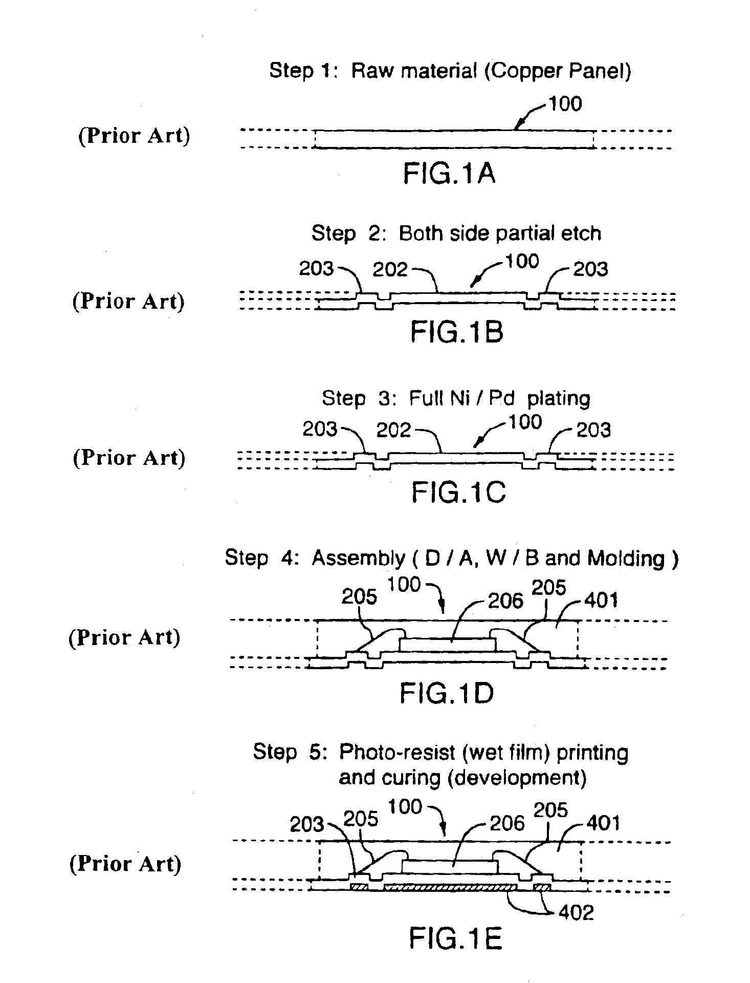
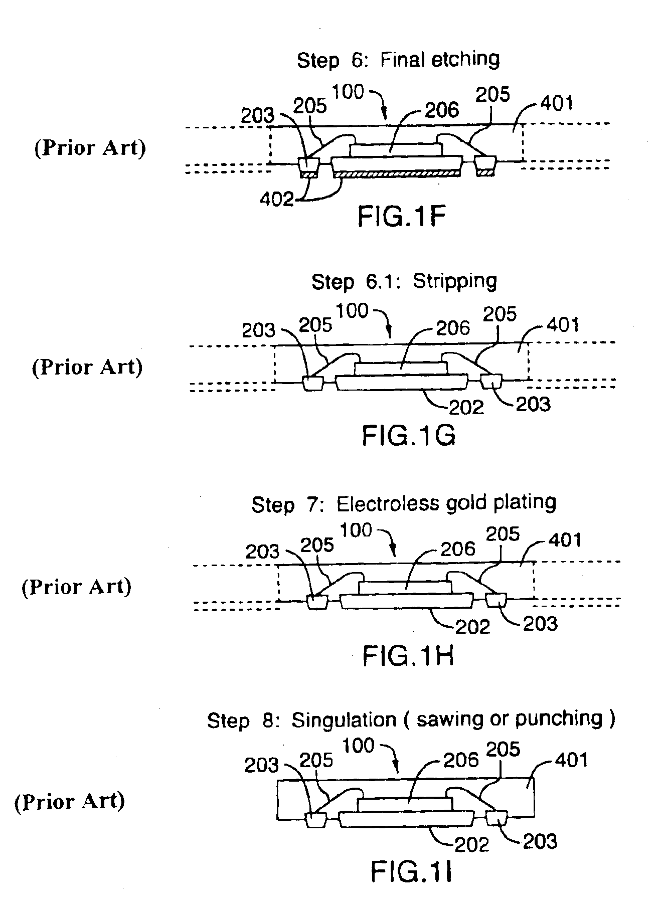
[0012]FIGS. 1A-1I show processing steps for manufacturing a Leadless Plastic Chip Carrier (LPCC) with top and bottom partial etch resulting in a bottom etch cavity, according to Applicants' prior art process;
second embodiment
[0013]FIGS. 2A-2G show processing steps for manufacturing a Leadless Plastic Chip Carrier (LPCC) with top and bottom partial etch incorporating standoff, according to Applicants' prior art process;
third embodiment
[0014]FIGS. 3A-3H show processing steps for manufacturing a Leadless Plastic Chip Carrier (LPCC) with top side partial etch and solder ball attachment, according to Applicants' prior art process;
Login to View More PUM
 Abstract
A leadless plastic chip carrier is constructed by half etching one or both sides of the package design onto a leadframe strip so as to create unique design features such as power and / or ground ring surrounding the die attach pad, interlocking rivet head construction for the contact pads, and an interlocking pattern for the die attach pad. After wire bonding and molding, a further etching is performed to isolate and expose contact pads. Singulation of individual chip packages from the leadframe strip is then performed by saw singulation or die punching.
Description
CROSS-REFERENCE TO RELATED APPLICATION[0001]This is a continuation-in-part of U.S. patent application Ser. No. 09 / 288,352, filed Apr. 8, 1999, now U.S. Pat. No. 6,498,099 which is a continuation-in-part of U.S. patent application Ser. No. 09 / 095,803, filed Jun. 10, 1998 now U.S. Pat. No. 6,229,200.FIELD OF THE INVENTION[0002]The present invention relates in general to integrated circuit packaging, and more particularly to an improved process for fabricating a leadless plastic chip carrier which includes a post mold etch back step and unique contact pad and die attach pad design features.BACKGROUND OF THE INVENTION[0003]According to well known prior art IC (integrated circuit) packaging methodologies, semiconductor dice are singulated and mounted using epoxy or other conventional means onto respective die pads (attach paddles) of a leadframe strip. Traditional QFP (Quad Flat Pack) packages incorporate inner leads which function as lands for wire bonding the semiconductor die bond pad...
Claims
Login to View More Application Information
Patent Timeline
 IPC IPC(8): H01L21/67H01L21/48H01L21/02H01L23/31H01L23/28H01L21/68H01L23/495H01L23/48H01L21/56
CPCH01L21/4832H01L21/561H01L21/568H01L23/3107H01L23/49541H01L23/49548H01L24/97H01L2221/68377H01L2224/1134H01L2224/48091H01L2224/48247H01L2924/01013H01L2924/01027H01L2924/01029H01L2924/01046H01L2924/01047H01L2924/01078H01L2924/01079H01L2924/01082H01L2924/14H01L2924/30107H01L2924/00014H01L24/48H01L2924/00013H01L2924/01005H01L2924/01006H01L2924/01033H01L2224/13099H01L2224/45144H01L2924/00H01L2924/15747H01L2924/181H01L24/45H01L2224/49433H01L2924/00015H01L2224/05599H01L2924/00012
InventorMCLELLAN, NEILFAN, CHUN HOTSANG, KWOK CHEUNGKWAN, KIN PUILAU, WING HIM
OwnerUTAC HEADQUARTERS PTE LTD